- 您现在的位置:买卖IC网 > PDF目录8680 > AD5323BRUZ-REEL (Analog Devices Inc)IC DAC 12BIT DUAL R-R 16-TSSOP PDF资料下载
参数资料
| 型号: | AD5323BRUZ-REEL |
| 厂商: | Analog Devices Inc |
| 文件页数: | 13/28页 |
| 文件大小: | 0K |
| 描述: | IC DAC 12BIT DUAL R-R 16-TSSOP |
| 产品培训模块: | Data Converter Fundamentals DAC Architectures |
| 标准包装: | 2,500 |
| 设置时间: | 8µs |
| 位数: | 12 |
| 数据接口: | 串行 |
| 转换器数目: | 2 |
| 电压电源: | 单电源 |
| 功率耗散(最大): | 2.5mW |
| 工作温度: | -40°C ~ 105°C |
| 安装类型: | 表面贴装 |
| 封装/外壳: | 16-TSSOP(0.173",4.40mm 宽) |
| 供应商设备封装: | 16-TSSOP |
| 包装: | 带卷 (TR) |
| 输出数目和类型: | 2 电压,单极;2 电压,双极 |
| 采样率(每秒): | 125k |
第1页第2页第3页第4页第5页第6页第7页第8页第9页第10页第11页第12页当前第13页第14页第15页第16页第17页第18页第19页第20页第21页第22页第23页第24页第25页第26页第27页第28页
AD5303/AD5313/AD5323
Rev. B | Page 20 of 28
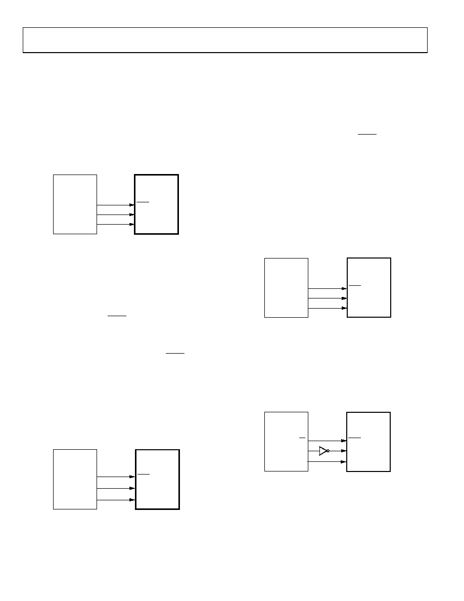
MICROPROCESSER INTERFACING
AD5303/AD5313/AD5323 TO ADSP-2101
INTERFACE
Figure 35 shows a serial interface between the AD5303/AD5313/
AD5323 and the ADSP-2101. The ADSP-2101 should be set up
to operate in the SPORT transmit alternate framing mode. The
ADSP-2101 sport is programmed through the SPORT control
register and should be configured as follows: internal clock
operation, active-low framing, 16-bit word length. Transmission
is initiated by writing a word to the Tx register after the SPORT
has been enabled.
SCLK
DIN
SYNC
TFS
DT
SCLK
*ADDITIONAL PINS OMITTED FOR CLARITY
00
47
2-
0
35
AD5303/
AD5313/
AD5323*
ADSP-2101
Figure 35. AD5303/AD5313/AD5323 to ADSP-2101 Interface
AD5303/AD5313/AD5323 TO 68HC11/68L11
INTERFACE
Figure 36 shows a serial interface between the AD5303/
AD5313/AD5323 and the 68HC11/68L11 microcontroller.
SCK of the 68HC11/68L11 drives the SCLK of the AD5303/
AD5313/AD5323, while the MOSI output drives the serial data
line (DIN) of the DAC. The SYNC signal is derived from a port
line (PC7). The setup conditions for correct operation of this
interface are as follows: the 68HC11/68L11 should be con-
figured so that its CPOL bit is a 0 and its CPHA bit is a 1.
When data is being transmitted to the DAC, the SYNC line
is taken low (PC7). When the 68HC11/68L11 is configured
as previously mentioned, data appearing on the MOSI output
is valid on the falling edge of SCK. Serial data from the 68HC11/
68L11 is transmitted in 8-bit bytes with only eight falling clock
edges occurring in the transmit cycle. Data is transmitted MSB
first. To load data to the AD5303/AD5313/ AD5323, PC7 is left
low after the first eight bits are transferred and a second serial
write operation is performed to the DAC; PC7 is taken high at
the end of this procedure.
DIN
SCLK
SYNC
PC7
SCK
MOSI
68HC11/68L11*
*ADDITIONAL PINS OMITTED FOR CLARITY
0
4
7
2
-0
3
6
AD5303/
AD5313/
AD5323*
Figure 36. AD5303/AD5313/AD5323 to 68HC11/68L11 Interface
AD5303/AD5313/AD5323 TO 80C51/80L51
INTERFACE
Figure 37 shows a serial interface between the AD5303/
AD5313/AD5323 and the 80C51/80L51 microcontroller. The
setup for the interface is as follows: TXD of the 80C51/80L51
drives SCLK of the AD5303/AD5313/AD5323, while RXD
drives the serial data line of the part. The SYNC signal is again
derived from a bit programmable pin on the port. In this case,
port line P3.3 is used. When data is to be transmitted to the
AD5303/AD5313/AD5323, P3.3 is taken low. The 80C51/80L51
transmits data only in 8-bit bytes; thus only eight falling clock
edges occur in the transmit cycle. To load data to the DAC, P3.3
is left low after the first eight bits are transmitted and a second
write cycle is initiated to transmit the second byte of data. P3.3
is taken high following the completion of this cycle. The 80C51/
80L51 output the serial data in a format that has the LSB first.
The AD5303/AD5313/AD5323 require data with MSB as the
first bit received. The 80C51/80L51 transmit routine should
take this into account.
DIN
SCLK
P3.3
TXD
RXD
80C51/80L51*
*ADDITIONAL PINS OMITTED FOR CLARITY.
00
47
2-
03
7
SYNC
AD5303/
AD5313/
AD5323*
Figure 37. AD5303/AD5313/AD5323 to 80C51/80L51 Interface
AD5303/AD5313/AD5323 TO MICROWIRE
INTERFACE
Figure 38 shows an interface between the AD5303/AD5313/
AD5323 and any MICROWIRE-compatible device. Serial
data is shifted out on the falling edge of the serial clock and
is clocked into the AD5303/AD5313/AD5323 on the rising
edge of the SK.
DIN
SCLK
SK
SO
MICROWIRE*
*ADDITIONAL PINS OMITTED FOR CLARITY.
00
47
2-
0
38
CS
SYNC
AD5303/
AD5313/
AD5323*
Figure 38. AD5303/AD5313/AD5323 to MICROWIRE Interface
相关PDF资料 |
PDF描述 |
|---|---|
| VE-J1X-MX-B1 | CONVERTER MINIMOD DC/DC 5.2V 75W |
| VI-J7Y-MY | CONVERTER MOD DC/DC 3.3V 33W |
| AD7224KRZ-18REEL | IC DAC 8BIT W/OUTPUT AMPS 18SOIC |
| LTC1450CN#PBF | IC D/A CONV 12BIT R-R PAR 24-DIP |
| LTC1450CN | IC D/A CONV 12BIT R-R PAR 24-DIP |
相关代理商/技术参数 |
参数描述 |
|---|---|
| AD5323BRUZ-REEL1 | 制造商:AD 制造商全称:Analog Devices 功能描述:2.5 V to 5.5 V, 230 ??A, Dual Rail-to-Rail Voltage Output 8-/10-/12-Bit DACs |
| AD5323BRUZ-REEL7 | 功能描述:IC DAC 12BIT DUAL R-R 16-TSSOP RoHS:是 类别:集成电路 (IC) >> 数据采集 - 数模转换器 系列:- 产品培训模块:LTC263x 12-, 10-, and 8-Bit VOUT DAC Family 特色产品:LTC2636 - Octal 12-/10-/8-Bit SPI VOUT DACs with 10ppm/°C Reference 标准包装:91 系列:- 设置时间:4µs 位数:10 数据接口:MICROWIRE?,串行,SPI? 转换器数目:8 电压电源:单电源 功率耗散(最大):2.7mW 工作温度:-40°C ~ 85°C 安装类型:表面贴装 封装/外壳:14-WFDFN 裸露焊盘 供应商设备封装:14-DFN-EP(4x3) 包装:管件 输出数目和类型:8 电压,单极 采样率(每秒):* |
| AD5323BRUZ-REEL71 | 制造商:AD 制造商全称:Analog Devices 功能描述:2.5 V to 5.5 V, 230 ??A, Dual Rail-to-Rail Voltage Output 8-/10-/12-Bit DACs |
| AD5323-EVAL | 制造商:Analog Devices 功能描述: |
| AD5324 | 制造商:AD 制造商全称:Analog Devices 功能描述:2.5 V to 5.5 V, 500 uA, Parallel Interface Quad Voltage-Output 8-/10-/12-Bit DACs |
发布紧急采购,3分钟左右您将得到回复。