- 您现在的位置:买卖IC网 > PDF目录10803 > AD5325BRM (Analog Devices Inc)IC DAC 12BIT 2WIRE I2C 10-MSOP PDF资料下载
参数资料
| 型号: | AD5325BRM |
| 厂商: | Analog Devices Inc |
| 文件页数: | 20/24页 |
| 文件大小: | 0K |
| 描述: | IC DAC 12BIT 2WIRE I2C 10-MSOP |
| 产品培训模块: | Data Converter Fundamentals DAC Architectures |
| 产品变化通告: | Product Discontinuance 27/Oct/2011 |
| 标准包装: | 50 |
| 设置时间: | 6µs |
| 位数: | 12 |
| 数据接口: | I²C,串行 |
| 转换器数目: | 4 |
| 电压电源: | 单电源 |
| 功率耗散(最大): | 5mW |
| 工作温度: | -40°C ~ 105°C |
| 安装类型: | 表面贴装 |
| 封装/外壳: | 10-TFSOP,10-MSOP(0.118",3.00mm 宽) |
| 供应商设备封装: | 10-MSOP |
| 包装: | 管件 |
| 输出数目和类型: | 4 电压,单极;4 电压,双极 |
| 采样率(每秒): | 125k |
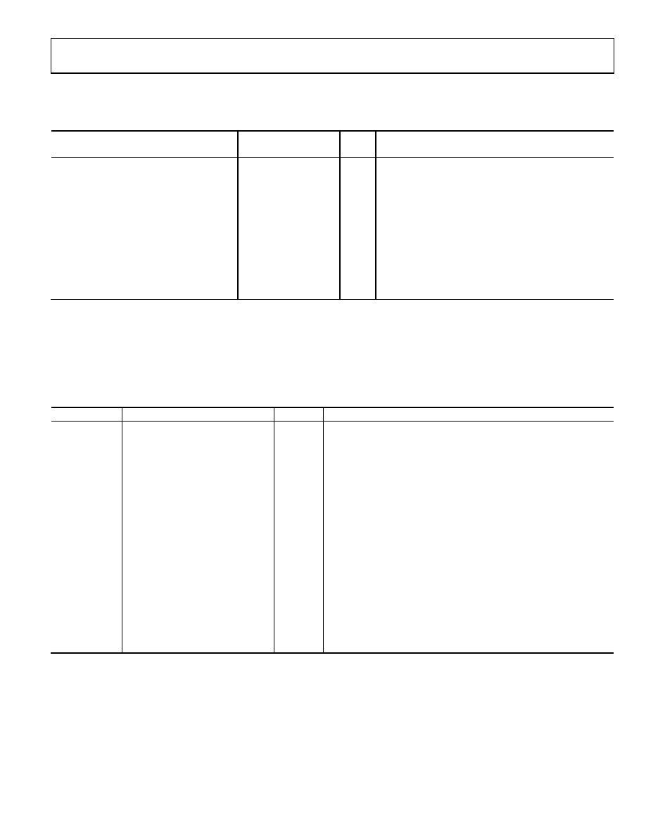
AD5305/AD5315/AD5325
Rev. G | Page 5 of 24
AC CHARACTERISTICS
VDD = 2.5 V to 5.5 V, RL = 2 kΩ to GND, CL = 200 pF to GND, all specifications TMIN to TMAX, unless otherwise noted.
Table 2.
A, B Version1
Parameter2, 3
Min
Typ
Max
Unit
Conditions/Comments
Output Voltage Settling Time
VREF = VDD = 5 V
AD5305
6
8
μs
scale to scale change (0×40 to 0×C0)
AD5315
7
9
μs
scale to scale change (0×100 to 0×300)
AD5325
8
10
μs
scale to scale change (0×400 to 0×C00)
Slew Rate
0.7
V/μs
Major-Code Transition Glitch Energy
12
nV-s
1 LSB change around major carry
Digital Feedthrough
1
nV-s
Digital Crosstalk
1
nV-s
DAC-to-DAC Crosstalk
3
nV-s
Multiplying Bandwidth
200
kHz
VREF = 2 V ± 0.1 V p-p
Total Harmonic Distortion
70
dB
VREF = 2.5 V ± 0.1 V p-p, frequency = 10 kHz
1 Temperature range (A, B version): 40°C to +105°C; typical at +25°C.
2 Guaranteed by design and characterization, not production tested.
3 See the Terminology section.
TIMING CHARACTERISTICS
VDD = 2.5 V to 5.5 V, all specifications TMIN to TMAX, unless otherwise noted.
Table 3.
Parameter1, 2
Limit at TMIN, TMAX (A, B Version)
Unit
Conditions/Comments
fSCL
400
kHz max
SCL clock frequency
t1
2.5
μs min
SCL cycle time
t2
0.6
μs min
tHIGH, SCL high time
t3
1.3
μs min
tLOW, SCL low time
t4
0.6
μs min
tHD,STA, start/repeated start condition hold time
t5
100
ns min
tSU,DAT, data setup time
t63
0.9
μs max
tHD,DAT, data hold time
0
μs min
tHD,DAT, data hold time
t7
0.6
μs min
tSU,STA, setup time for repeated start
t8
0.6
μs min
tSU,STO, stop condition setup time
t9
1.3
μs min
tBUF, bus-free time between a stop and a start condition
t10
300
ns max
tR, rise time of SCL and SDA when receiving
0
ns min
tR, rise time of SCL and SDA when receiving (CMOS compatible)
t11
250
ns max
tF, fall time of SDA when transmitting
0
ns min
tF, fall time of SDA when receiving (CMOS compatible)
300
ns max
tF, fall time of SCL and SDA when receiving
20 + 0.1 CB4
ns min
tF, fall time of SCL and SDA when transmitting
CB4
400
pF max
Capacitive load for each bus line
1 See Figure 2.
2 Guaranteed by design and characterization; not production tested.
3 A master device must provide a hold time of at least 300 ns for the SDA signal (referred to VIH min of the SCL signal) in order to bridge the undefined region of SCL’s
falling edge.
4 CB is the total capacitance of one bus line in pF. tR and tF measured between 0.3 VDD and 0.7 VDD.
相关PDF资料 |
PDF描述 |
|---|---|
| AD5324BRM-REEL | IC DAC 12BIT QUAD VOUT 10-MSOP |
| LTC2850HS8#PBF | IC TXRX RS485 20MBPS 8-SOIC |
| BA2903HFVM-CTR | IC COMPARATOR DUAL 36V MSOP-8 |
| KSZ8041TL | TRANSCEIVER 10/100BASE 48-TQFP |
| LTC2804CGN-1#PBF | IC TXRX RS232 DUAL 16-SSOP |
相关代理商/技术参数 |
参数描述 |
|---|---|
| AD5325BRM-REEL | 功能描述:IC DAC 12BIT 2WIRE I2C 10-MSOP RoHS:否 类别:集成电路 (IC) >> 数据采集 - 数模转换器 系列:- 标准包装:47 系列:- 设置时间:2µs 位数:14 数据接口:并联 转换器数目:1 电压电源:单电源 功率耗散(最大):55µW 工作温度:-40°C ~ 85°C 安装类型:表面贴装 封装/外壳:28-SSOP(0.209",5.30mm 宽) 供应商设备封装:28-SSOP 包装:管件 输出数目和类型:1 电流,单极;1 电流,双极 采样率(每秒):* |
| AD5325BRM-REEL7 | 功能描述:IC DAC 12BIT 2WIRE I2C 10-MSOP RoHS:否 类别:集成电路 (IC) >> 数据采集 - 数模转换器 系列:- 标准包装:47 系列:- 设置时间:2µs 位数:14 数据接口:并联 转换器数目:1 电压电源:单电源 功率耗散(最大):55µW 工作温度:-40°C ~ 85°C 安装类型:表面贴装 封装/外壳:28-SSOP(0.209",5.30mm 宽) 供应商设备封装:28-SSOP 包装:管件 输出数目和类型:1 电流,单极;1 电流,双极 采样率(每秒):* |
| AD5325BRMZ | 功能描述:IC DAC 12BIT 2WIRE I2C 10-MSOP RoHS:是 类别:集成电路 (IC) >> 数据采集 - 数模转换器 系列:- 产品培训模块:Lead (SnPb) Finish for COTS Obsolescence Mitigation Program 标准包装:50 系列:- 设置时间:4µs 位数:12 数据接口:串行 转换器数目:2 电压电源:单电源 功率耗散(最大):- 工作温度:-40°C ~ 85°C 安装类型:表面贴装 封装/外壳:8-TSSOP,8-MSOP(0.118",3.00mm 宽) 供应商设备封装:8-uMAX 包装:管件 输出数目和类型:2 电压,单极 采样率(每秒):* 产品目录页面:1398 (CN2011-ZH PDF) |
| AD5325BRMZ1 | 制造商:AD 制造商全称:Analog Devices 功能描述:2.5 V to 5.5 V, 500 ??A, 2-Wire Interface Interface |
| AD5325BRMZ-REEL | 功能描述:IC DAC 12BIT 2WIRE I2C 10MSOP RoHS:是 类别:集成电路 (IC) >> 数据采集 - 数模转换器 系列:- 标准包装:47 系列:- 设置时间:2µs 位数:14 数据接口:并联 转换器数目:1 电压电源:单电源 功率耗散(最大):55µW 工作温度:-40°C ~ 85°C 安装类型:表面贴装 封装/外壳:28-SSOP(0.209",5.30mm 宽) 供应商设备封装:28-SSOP 包装:管件 输出数目和类型:1 电流,单极;1 电流,双极 采样率(每秒):* |
发布紧急采购,3分钟左右您将得到回复。