参数资料
| 型号: | AD5334BRUZ |
| 厂商: | Analog Devices Inc |
| 文件页数: | 17/20页 |
| 文件大小: | 0K |
| 描述: | IC DAC 8BIT QUAD VOUT 24-TSSOP |
| 产品培训模块: | Data Converter Fundamentals DAC Architectures |
| 标准包装: | 62 |
| 设置时间: | 6µs |
| 位数: | 8 |
| 数据接口: | 并联 |
| 转换器数目: | 4 |
| 电压电源: | 单电源 |
| 功率耗散(最大): | 4.5mW |
| 工作温度: | -40°C ~ 105°C |
| 安装类型: | 表面贴装 |
| 封装/外壳: | 24-TSSOP(0.173",4.40mm 宽) |
| 供应商设备封装: | 24-TSSOP |
| 包装: | 管件 |
| 输出数目和类型: | 4 电压,单极;4 电压,双极 |
| 采样率(每秒): | 167k |
| 产品目录页面: | 782 (CN2011-ZH PDF) |
REV. 0
AD5334/AD5335/AD5336/AD5344
–6–
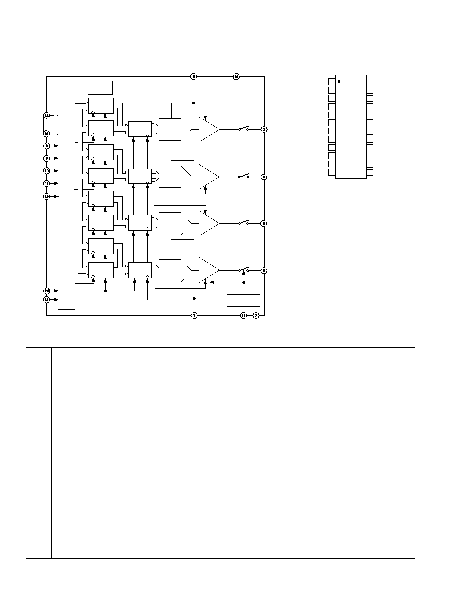
AD5335 FUNCTIONAL BLOCK DIAGRAM
.
VOUTA
BUFFER
GND
AD5335
VOUTB
VOUTC
VOUTD
TO ALL DACS
AND BUFFERS
POWER-DOWN
LOGIC
PD
DAC
REGISTER
VREFC/D
INTER-
FACE
LOGIC
VDD
VREFA/B
HBEN
DB7
DB0
CS
WR
A0
A1
CLR
LDAC
RESET
POWER-ON
RESET
HIGH BYTE
REGISTER
BUFFER
DAC
REGISTER
DAC
REGISTER
DAC
REGISTER
LOW BYTE
REGISTER
HIGH BYTE
REGISTER
HIGH BYTE
REGISTER
HIGH BYTE
REGISTER
LOW BYTE
REGISTER
LOW BYTE
REGISTER
LOW BYTE
REGISTER
10-BIT
DAC
10-BIT
DAC
10-BIT
DAC
10-BIT
DAC
AD5335 PIN FUNCTION DESCRIPTIONS
Pin
No.
Mnemonic
Function
1VREFC/D
Unbuffered Reference Input for DACs C and D.
2VREFA/B
Unbuffered Reference Input for DACs A and B.
3VOUTA
Output of DAC A. Buffered output with rail-to-rail operation.
4VOUTB
Output of DAC B. Buffered output with rail-to-rail operation.
5VOUTC
Output of DAC C. Buffered output with rail-to-rail operation.
6VOUTD
Output of DAC D. Buffered output with rail-to-rail operation.
7
GND
Ground Reference Point for All Circuitry on the Part.
8
CS
Active Low Chip Select Input. This is used in conjunction with
WR to write data to the parallel interface.
9
WR
Active Low Write Input. This is used in conjunction with
CS to write data to the parallel interface.
10
A0
LSB Address Pin for Selecting which DAC Is to Be Written to.
11
A1
MSB Address Pin for Selecting which DAC Is to Be Written to.
12
LDAC
Active Low Control Input that Updates the DAC Registers with the Contents of the Input Registers.
This allows all DAC outputs to be simultaneously updated.
13
PD
Power-Down Pin. This active low control pin puts all DACs into power-down mode.
14
VDD
Power Supply Pin. This part can operate from 2.5 V to 5.5 V and the supply should be decoupled with a
10
F capacitor in parallel with a 0.1 F capacitor to GND.
15–22
DB0–DB7
Eight Parallel Data Inputs. DB7 is the MSB of these eight bits.
23
HBEN
This pin is used when writing to the device to determine if data is written to the high byte register or the
low byte register.
24
CLR
Asynchronous Active Low Control Input that Clears All Input Registers and DAC Registers to Zeros.
AD5335 PIN CONFIGURATION
TOP VIEW
(Not to Scale)
24
23
22
21
20
19
18
17
16
15
14
13
1
2
3
4
5
6
7
8
9
10
11
12
AD5335
LDAC
A1
A0
WR
CS
VREFC/D
VREFA/B
VOUTA
VOUTB
GND
VOUTD
VOUTC
PD
VDD
DB0
DB1
DB2
CLR
HBEN
DB7
DB6
DB3
DB4
DB5
10-BIT
相关PDF资料 |
PDF描述 |
|---|---|
| VE-J4M-MZ-F3 | CONVERTER MOD DC/DC 10V 25W |
| LTC2627IDE-1#PBF | IC DAC 12BIT R-R I2C 12-DFN |
| SY89321LMG TR | IC TRANSLATOR LVPECL-LVTTL 8-MLF |
| VE-J4M-MZ-F1 | CONVERTER MOD DC/DC 10V 25W |
| M83723/96G14077 | CONN PLUG 7POS STRAIGHT W/PINS |
相关代理商/技术参数 |
参数描述 |
|---|---|
| AD5334BRUZ-REEL | 功能描述:IC DAC 8BIT QUAD VOUT 24TSSOP RoHS:是 类别:集成电路 (IC) >> 数据采集 - 数模转换器 系列:- 标准包装:2,400 系列:- 设置时间:- 位数:18 数据接口:串行 转换器数目:3 电压电源:模拟和数字 功率耗散(最大):- 工作温度:-40°C ~ 85°C 安装类型:表面贴装 封装/外壳:36-TFBGA 供应商设备封装:36-TFBGA 包装:带卷 (TR) 输出数目和类型:* 采样率(每秒):* |
| AD5334BRUZ-REEL7 | 功能描述:IC DAC 8BIT QUAD VOUT 24TSSOP RoHS:是 类别:集成电路 (IC) >> 数据采集 - 数模转换器 系列:- 产品培训模块:LTC263x 12-, 10-, and 8-Bit VOUT DAC Family 特色产品:LTC2636 - Octal 12-/10-/8-Bit SPI VOUT DACs with 10ppm/°C Reference 标准包装:91 系列:- 设置时间:4µs 位数:10 数据接口:MICROWIRE?,串行,SPI? 转换器数目:8 电压电源:单电源 功率耗散(最大):2.7mW 工作温度:-40°C ~ 85°C 安装类型:表面贴装 封装/外壳:14-WFDFN 裸露焊盘 供应商设备封装:14-DFN-EP(4x3) 包装:管件 输出数目和类型:8 电压,单极 采样率(每秒):* |
| AD5335 | 制造商:AD 制造商全称:Analog Devices 功能描述:2.5 V to 5.5 V, 500 uA, Parallel Interface Quad Voltage-Output 8-/10-/12-Bit DACs |
| AD5335BRU | 制造商:Analog Devices 功能描述:DAC 4-CH Resistor-String 10-bit 24-Pin TSSOP 制造商:Rochester Electronics LLC 功能描述:10-BIT,QUAD BYTE DAC, I.C - Bulk 制造商:Analog Devices 功能描述:10BIT DAC QUAD SMD 5335 TSSOP24 |
| AD5335BRU-REEL | 制造商:Analog Devices 功能描述:DAC 4-CH Resistor-String 10-bit 24-Pin TSSOP T/R |
发布紧急采购,3分钟左右您将得到回复。