- 您现在的位置:买卖IC网 > PDF目录8689 > AD5336BRUZ-REEL7 (Analog Devices Inc)IC DAC 10BIT QUAD VOUT 28-TSSOP PDF资料下载
参数资料
| 型号: | AD5336BRUZ-REEL7 |
| 厂商: | Analog Devices Inc |
| 文件页数: | 9/20页 |
| 文件大小: | 0K |
| 描述: | IC DAC 10BIT QUAD VOUT 28-TSSOP |
| 产品培训模块: | Data Converter Fundamentals DAC Architectures |
| 标准包装: | 1,000 |
| 设置时间: | 7µs |
| 位数: | 10 |
| 数据接口: | 并联 |
| 转换器数目: | 4 |
| 电压电源: | 单电源 |
| 功率耗散(最大): | 4.5mW |
| 工作温度: | -40°C ~ 105°C |
| 安装类型: | 表面贴装 |
| 封装/外壳: | 28-TSSOP(0.173",4.40mm 宽) |
| 供应商设备封装: | 28-TSSOP |
| 包装: | 带卷 (TR) |
| 输出数目和类型: | 4 电压,单极;4 电压,双极 |
| 采样率(每秒): | 143k |
REV. 0
AD5334/AD5335/AD5336/AD5344
–17–
Decoding Multiple AD5334/AD5335/AD5336/AD5344
The
CS pin on these devices can be used in applications to decode
a number of DACs. In this application, all DACs in the system
receive the same data and
WR pulses, but only the CS to one of
the DACs will be active at any one time, so data will only be
written to the DAC whose
CS is low. If multiple AD5343s are
being used, a common HBEN line will also be required to
determine if the data is written to the high-byte or low-byte
register of the selected DAC.
The 74HC139 is used as a 2- to 4-line decoder to address any
of the DACs in the system. To prevent timing errors from oc-
curring, the enable input should be brought to its inactive state
while the coded address inputs are changing state. Figure 36 shows
a diagram of a typical setup for decoding multiple devices in a
system. Once data has been written sequentially to all DACs in
a system, all the DACs can be updated simultaneously using a
common
LDAC line. A common CLR line can also be used to
reset all DAC outputs to zero (except on the AD5344).
ENABLE
CODED
ADDRESS
1G
1A
1B
VDD
VCC
74HC139
DGND
1Y0
1Y1
1Y2
1Y3
A0
A1
HBEN
WR
LDAC
CLR
DATA
INPUTS
DATA
INPUTS
DATA
INPUTS
A1
A0
HBEN*
WR
LDAC
CLR
CS
DATA
INPUTS
DATA
BUS
*AD5335 ONLY
A1
A0
HBEN*
WR
LDAC
CLR
CS
A1
A0
HBEN*
WR
LDAC
CLR
CS
A1
A0
HBEN*
WR
LDAC
CLR
CS
AD5334/AD5335/
AD5336/AD5344
AD5334/AD5335/
AD5336/AD5344
AD5334/AD5335/
AD5336/AD5344
AD5334/AD5335/
AD5336/AD5344
Figure 36. Decoding Multiple DAC Devices
AD5334/AD5335/AD5336/AD5344 as a Digitally Programmable
Window Detector
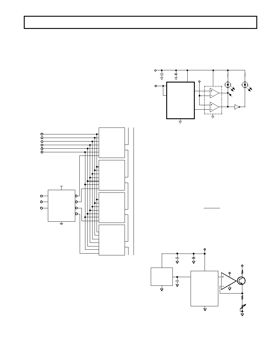
A digitally programmable upper/lower limit detector using two
of the DACs in the AD5334/AD5335/AD5336/AD5344 is
shown in Figure 37.
Any pair of DACs in the device may be used, but for simplicity
the description will refer to DACs A and B.
Care must be taken to connect the correct reference inputs to
the reference source. The AD5334 and AD5335 have only two
reference inputs, VREFA/B for DACs A and B and VREFC/D for
DACs C and D. If DACs A and B are used (for example) then
only VREFA/B is needed. DACs C and D and VREFC/D may be
used for some other purpose. The AD5336 and AD5344 have
separate reference inputs for each DAC.
The upper and lower limits for the test are loaded to DACs A
and B which, in turn, set the limits on the CMP04. If a signal at
the VIN input is not within the programmed window, an LED
will indicate the fail condition.
5V
0.1 F
10 F
AD5336/AD5344
GND
VREFA
VDD
VOUTA
VREFB
VOUTB
VIN
FAIL
PASS
1k
PASS/
FAIL
1/6 74HC05
1/2
CMP04
VREF
Figure 37. Programmable Window Detector
Programmable Current Source
Figure 38 shows the AD5334/AD5335/AD5336/AD5344 used
as the control element of a programmable current source. In this
example, the full-scale current is set to 1 mA. The output volt-
age from the DAC is applied across the current setting resistor
of 4.7 k
in series with the 470 adjustment potentiometer,
which gives an adjustment of about
±5%. Suitable transistors to
place in the feedback loop of the amplier include the BC107
and the 2N3904, which enable the current source to operate
from a minimum VSOURCE of 6 V. The operating range is deter-
mined by the operating characteristics of the transistor. Suitable
ampliers include the AD820 and the OP295, both having rail-
to-rail operation on their outputs. The current for any digital
input code and resistor value can be calculated as follows:
IG
V
D
R
mA
REF
N
=×
×
()
2
Where:
G is the gain of the buffer amplier (1 or 2)
D is the digital input code
N is the DAC resolution (8, 10, or 12 bits)
R is the sum of the resistor plus adjustment potentiometer in k
AD5334/AD5335/
AD5336/AD5344
GND
VDD = 5V
EXT
REF
VOUT*
AD780/REF192
WITH VDD = 5V
GND
VIN
VOUT
VREF*
VDD
4.7k
5V
*ONLY ONE CHANNEL OF VREF AND VOUT SHOWN
0.1 F
10 F
470
LOAD
VSOURCE
AD820/
OP295
Figure 38. Programmable Current Source
相关PDF资料 |
PDF描述 |
|---|---|
| V48A12H500BL3 | CONVERTER MOD DC/DC 12V 500W |
| V48A12H500BL | CONVERTER MOD DC/DC 12V 500W |
| PI49FCT3807DHE | IC CLK BUFF 1:10 156MHZ 20-SSOP |
| MC10EL11DTR2G | IC CLK BUFFER 1:2 1.5GHZ 8-TSSOP |
| LTC1451CS8 | IC D/A CONV 12BIT R-R 8-SOIC |
相关代理商/技术参数 |
参数描述 |
|---|---|
| AD5337 | 制造商:AD 制造商全称:Analog Devices 功能描述:2.5 V to 5.5 V, 250 UA, 2-Wire Interface Dual-Voltage Output, 8-/10-/12-Bit DACs |
| AD5337ARM | 功能描述:IC DAC 8BIT DUAL 2-WIRE 8-MSOP RoHS:否 类别:集成电路 (IC) >> 数据采集 - 数模转换器 系列:- 产品培训模块:Data Converter Fundamentals DAC Architectures 设计资源:Unipolar, Precision DC Digital-to-Analog Conversion using AD5450/1/2/3 8-14-Bit DACs (CN0052) Precision, Bipolar, Configuration for AD5450/1/2/3 8-14bit Multiplying DACs (CN0053) AC Signal Processing Using AD5450/1/2/3 Current Output DACs (CN0054) Programmable Gain Element Using AD5450/1/2/3 Current Output DAC Family (CN0055) Single Supply Low Noise LED Current Source Driver Using a Current Output DAC in the Reverse Mode (CN0139) 标准包装:10,000 系列:- 设置时间:- 位数:12 数据接口:DSP,MICROWIRE?,QSPI?,串行,SPI? 转换器数目:1 电压电源:单电源 功率耗散(最大):- 工作温度:-40°C ~ 125°C 安装类型:表面贴装 封装/外壳:SOT-23-8 薄型,TSOT-23-8 供应商设备封装:TSOT-23-8 包装:带卷 (TR) 输出数目和类型:1 电流,单极;1 电流,双极 采样率(每秒):2.7M |
| AD5337ARM-REEL7 | 功能描述:IC DAC 8BIT DUAL 2-WIRE 8MSOP TR RoHS:否 类别:集成电路 (IC) >> 数据采集 - 数模转换器 系列:- 标准包装:2,400 系列:- 设置时间:- 位数:18 数据接口:串行 转换器数目:3 电压电源:模拟和数字 功率耗散(最大):- 工作温度:-40°C ~ 85°C 安装类型:表面贴装 封装/外壳:36-TFBGA 供应商设备封装:36-TFBGA 包装:带卷 (TR) 输出数目和类型:* 采样率(每秒):* |
| AD5337ARMZ | 功能描述:IC DAC 8BIT DUAL 2-WIRE 8-MSOP RoHS:是 类别:集成电路 (IC) >> 数据采集 - 数模转换器 系列:- 产品培训模块:Data Converter Fundamentals DAC Architectures 标准包装:3,000 系列:nanoDAC™ 设置时间:80µs 位数:18 数据接口:DSP,MICROWIRE?,QSPI?,串行,SPI? 转换器数目:1 电压电源:单电源 功率耗散(最大):- 工作温度:-40°C ~ 105°C 安装类型:表面贴装 封装/外壳:SOT-23-8 供应商设备封装:SOT-23-8 包装:带卷 (TR) 输出数目和类型:1 电压,单极 采样率(每秒):- 产品目录页面:784 (CN2011-ZH PDF) 配用:EVAL-AD5680EBZ-ND - BOARD EVAL FOR AD5680 其它名称:AD5680BRJZ-2REEL7TR |
| AD5337ARMZ1 | 制造商:AD 制造商全称:Analog Devices 功能描述:2.5 V to 5.5 V, 250 muA, 2-Wire Interface |
发布紧急采购,3分钟左右您将得到回复。