- 您现在的位置:买卖IC网 > PDF目录373878 > AD5339BRM-REEL (ANALOG DEVICES INC) 2.5 V to 5.5 V, 250 UA, 2-Wire Interface Dual-Voltage Output, 8-/10-/12-Bit DACs PDF资料下载
参数资料
| 型号: | AD5339BRM-REEL |
| 厂商: | ANALOG DEVICES INC |
| 元件分类: | DAC |
| 英文描述: | 2.5 V to 5.5 V, 250 UA, 2-Wire Interface Dual-Voltage Output, 8-/10-/12-Bit DACs |
| 中文描述: | SERIAL INPUT LOADING, 8 us SETTLING TIME, 12-BIT DAC, PDSO8 |
| 封装: | MO-187AA, MSOP-8 |
| 文件页数: | 6/24页 |
| 文件大小: | 654K |
| 代理商: | AD5339BRM-REEL |
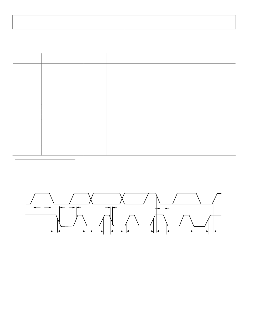
AD5337/AD5338/AD5339
TIMING CHARACTERISTICS
V
DD
= 2.5 V to 5.5 V. All specifications T
MIN
to T
MAX
, unless otherwise noted.
Table 3.
Limit at T
MIN
, T
MAX
(A and B Versions)
f
SCL
400
t
1
2.5
t
2
0.6
t
3
1.3
t
4
0.6
t
5
100
t
61
0.9
0
t
7
0.6
t
8
0.6
t
9
1.3
t
10
300
0
t
11
250
0
300
20 + 0.1 C
B2
C
B
400
Rev. A | Page 6 of 24
Parameter
Unit
kHz max
μs min
μs min
μs min
μs min
ns min
μs max
μs min
μs min
μs min
μs min
ns max
ns min
ns max
ns min
ns max
ns min
pF max
Conditions/Comments
SCL clock frequency
SCL cycle time
t
HIGH
, SCL high time
t
LOW
, SCL low time
t
HD,
STA
, start/repeated start condition hold time
t
SU,
DAT
, data setup time
t
HD,
DAT
, data hold time
t
HD,
DAT
, data hold time
t
SU,
STA
, setup time for repeated start
t
SU,
STO
, stop condition setup time
t
BUF
, bus free time between a stop and a start condition
t
R
, rise time of SCL and SDA when receiving
t
R
, rise time of SCL and SDA when receiving (CMOS-compatible)
t
F
, fall time of SDA when transmitting
t
F
, fall time of SDA when receiving (CMOS-compatible)
t
F
, fall time of SCL and SDA when receiving
t
F
, fall time of SCL and SDA when transmitting
Capacitive load for each bus line
1
A master device must provide a hold time of at least 300 ns for the SDA signal (referred to V
IH
min of the SCL signal) in order to bridge the undefined region of SCL’s
falling edge.
2
C
B
is the total capacitance of one bus line in pF; t
R
and t
F
measured between 0.3 V
DD
and 0.7 V
DD
.
STOP
SCL
SDA
START
CONDITION
t
9
t
3
t
4
t
6
t
2
t
5
t
7
t
8
t
1
t
4
t
11
t
10
REPEATED
START
CONDITION
CONDITION
0
Figure 2. 2-Wire Serial Interface Timing Diagram
相关PDF资料 |
PDF描述 |
|---|---|
| AD5339BRM-REEL7 | 2.5 V to 5.5 V, 250 UA, 2-Wire Interface Dual-Voltage Output, 8-/10-/12-Bit DACs |
| AD534K | Dual 14-bit 105MSPS ADC with serialized LVDS output 48-VQFN -40 to 85 |
| AD534KD | Dual 14-bit 125MSPS ADC with serialized LVDS output 48-VQFN -40 to 85 |
| AD534KH | Dual 14-bit 125MSPS ADC with serialized LVDS output 48-VQFN -40 to 85 |
| AD534L | Dual 14-bit 125MSPS ADC with serialized LVDS output 48-VQFN -40 to 85 |
相关代理商/技术参数 |
参数描述 |
|---|---|
| AD5339BRM-REEL7 | 制造商:Analog Devices 功能描述:DAC 2-CH Resistor-String 12-bit 8-Pin MSOP T/R 制造商:Analog Devices 功能描述:DAC 2CH RES-STRING 12-BIT 8MSOP - Tape and Reel |
| AD5339BRMZ | 功能描述:IC DAC 12BIT DUAL 2-WIRE 8-MSOP RoHS:是 类别:集成电路 (IC) >> 数据采集 - 数模转换器 系列:- 标准包装:1 系列:- 设置时间:4.5µs 位数:12 数据接口:串行,SPI? 转换器数目:1 电压电源:单电源 功率耗散(最大):- 工作温度:-40°C ~ 125°C 安装类型:表面贴装 封装/外壳:8-SOIC(0.154",3.90mm 宽) 供应商设备封装:8-SOICN 包装:剪切带 (CT) 输出数目和类型:1 电压,单极;1 电压,双极 采样率(每秒):* 其它名称:MCP4921T-E/SNCTMCP4921T-E/SNRCTMCP4921T-E/SNRCT-ND |
| AD5339BRMZ-REEL | 功能描述:IC DAC 12BIT DUAL 2-WIRE 8-MSOP RoHS:是 类别:集成电路 (IC) >> 数据采集 - 数模转换器 系列:- 标准包装:47 系列:- 设置时间:2µs 位数:14 数据接口:并联 转换器数目:1 电压电源:单电源 功率耗散(最大):55µW 工作温度:-40°C ~ 85°C 安装类型:表面贴装 封装/外壳:28-SSOP(0.209",5.30mm 宽) 供应商设备封装:28-SSOP 包装:管件 输出数目和类型:1 电流,单极;1 电流,双极 采样率(每秒):* |
| AD5339BRMZ-REEL7 | 功能描述:IC DAC 12BIT DUAL 2-WIRE 8-MSOP RoHS:是 类别:集成电路 (IC) >> 数据采集 - 数模转换器 系列:- 标准包装:47 系列:- 设置时间:2µs 位数:14 数据接口:并联 转换器数目:1 电压电源:单电源 功率耗散(最大):55µW 工作温度:-40°C ~ 85°C 安装类型:表面贴装 封装/外壳:28-SSOP(0.209",5.30mm 宽) 供应商设备封装:28-SSOP 包装:管件 输出数目和类型:1 电流,单极;1 电流,双极 采样率(每秒):* |
| AD533JD | 制造商:Rochester Electronics LLC 功能描述:- Bulk |
发布紧急采购,3分钟左右您将得到回复。