- 您现在的位置:买卖IC网 > PDF目录8662 > AD5347BRU-REEL (Analog Devices Inc)IC DAC 10BIT OCTAL VOUT 38-TSSOP PDF资料下载
参数资料
| 型号: | AD5347BRU-REEL |
| 厂商: | Analog Devices Inc |
| 文件页数: | 8/24页 |
| 文件大小: | 0K |
| 描述: | IC DAC 10BIT OCTAL VOUT 38-TSSOP |
| 产品培训模块: | Data Converter Fundamentals DAC Architectures |
| 标准包装: | 2,500 |
| 设置时间: | 7µs |
| 位数: | 10 |
| 数据接口: | 并联 |
| 转换器数目: | 8 |
| 电压电源: | 单电源 |
| 功率耗散(最大): | 8.3mW |
| 工作温度: | -40°C ~ 105°C |
| 安装类型: | 表面贴装 |
| 封装/外壳: | 38-TFSOP(0.173",4.40mm 宽) |
| 供应商设备封装: | 38-TSSOP |
| 包装: | 带卷 (TR) |
| 输出数目和类型: | 8 电压,单极;8 电压,双极 |
| 采样率(每秒): | 143k |
AD5346/AD5347/AD5348
Rev. 0 | Page 16 of 24
FUNCTIONAL DESCRIPTION
The AD5346/AD5347/AD5348 are octal resistor-string DACs
fabricated by a CMOS process with resolutions of 8, 10, and 12
bits, respectively. They are written to using a parallel interface.
They operate from single supplies of 2.5 V to 5.5 V, and the
output buffer amplifiers offer rail-to-rail output swing. The gain
of the buffer amplifiers can be set to 1 or 2 to give an output
voltage range of 0 V to VREF or 0 V to 2 × VREF. The AD5346/
AD5347/AD5348 have reference inputs that may be buffered to
draw virtually no current from the reference source. The devices
have a power-down feature that reduces current consumption
to only 100 nA @ 3 V.
DIGITAL-TO-ANALOG SECTION
The architecture of one DAC channel consists of a reference
buffer and a resistor-string DAC followed by an output buffer
amplifier. The voltage at the VREF pin provides the reference
voltage for the DAC. Figure 37 shows a block diagram of the
DAC architecture. Because the input coding to the DAC is
straight binary, the ideal output voltage is given by
Gain
D
V
N
REF
OUT
×
=
2
where:
D
is the decimal equivalent of the binary code, which is loaded
to the DAC register:
0–255 for AD5346 (8 bits)
0–1023 for AD5347 (10 bits)
0–4095 for AD5348 (12 bits)
N
is the DAC resolution.
Gain
is the output amplifier gain (1 or 2).
VOUTA
(GAIN = +1 OR +2)
VREFAB
BUF
DAC
REGISTER
INPUT
REGISTER
RESISTOR
STRING
OUTPUT
BUFFER AMPLIFIER
REFERENCE
BUFFER
03331-
0-
020
Figure 37. Single DAC Channel Architecture
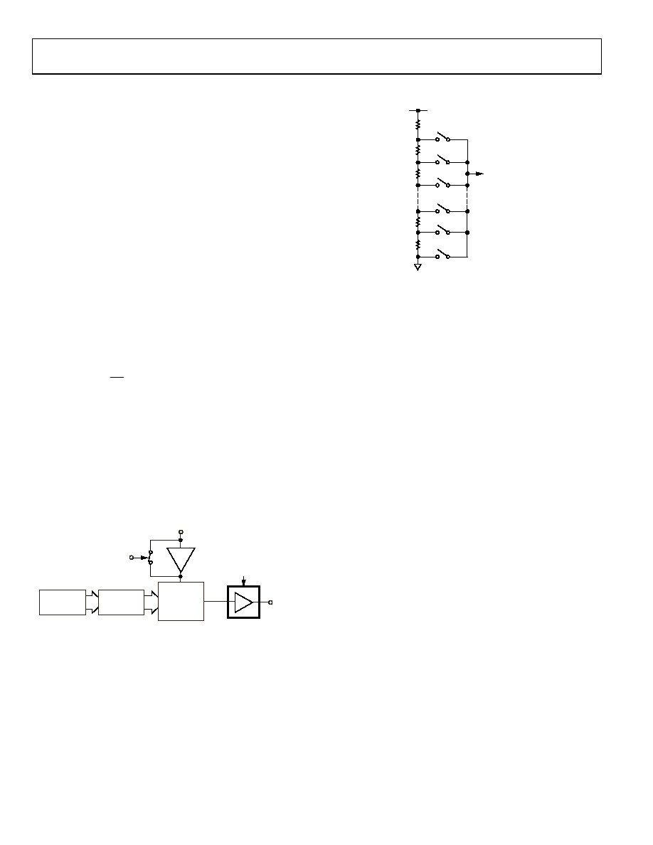
RESISTOR STRING
The resistor string section is shown in Figure 38. It is simply a
string of resistors, each of value R. The digital code loaded to
the DAC register determines at what node on the string the
voltage is tapped off to be fed into the output amplifier. The
voltage is tapped off by closing one of the switches connecting
the string to the amplifier. Because it is a string of resistors, it is
guaranteed monotonic.
TO OUTPUT
AMPLIFIER
R
VREF
03331-0-021
Figure 38. Resistor String
DAC REFERENCE INPUT
The DACs operate with an external reference. The AD5346/
AD5347/AD5348 have a reference input for each pair of DACs.
The reference inputs may be configured as buffered or
unbuffered. This option is controlled by the BUF pin.
In buffered mode (BUF = 1), the current drawn from an
external reference voltage is virtually zero because the imped-
ance is at least 10 M. The reference input range is 1 V to VDD.
In unbuffered mode (BUF = 0), the user can have a reference
voltage as low as 0.25 V and as high as VDD because there is no
restriction due to headroom and footroom of the reference
amplifier. The impedance is still large at typically 90 k for 0 V
to VREF mode and 45 k for 0 V to 2 × VREF mode.
If using an external buffered reference (such as REF192), there
is no need to use the on-chip buffer.
OUTPUT AMPLIFIER
The output buffer amplifier is capable of generating output
voltages to within 1 mV of either rail. Its actual range depends
on VREF, GAIN, the load on VOUT, and offset error.
If a gain of +1 is selected (GAIN = 0), the output range is
0.001 V to VREF.
If a gain of +2 is selected (GAIN = +1), the output range is
0.001 V to 2 × VREF. However, because of clamping, the
maximum output is limited to VDD – 0.001 V.
The output amplifier is capable of driving a load of 2 k to
GND or VDD, in parallel with 500 pF to GND or VDD. The source
and sink capabilities of the output amplifier can be seen in
The slew rate is 0.7 V/s with a half-scale settling time to ±0.5 LSB
(at 8 bits) of 6 s with the output unloaded. See Figure 29.
相关PDF资料 |
PDF描述 |
|---|---|
| VE-J7J-MX-B1 | CONVERTER MOD DC/DC 36V 75W |
| LTC8143ESW#TR | IC DAC 12BIT SERIAL MULTI 16SOIC |
| LTC2624IGN-1#TRPBF | IC DAC 12BIT QUAD R-R OUT 16SSOP |
| LTC2624IGN#TRPBF | IC DAC 12BIT QUAD R-R OUT 16SSOP |
| VE-J72-MX-B1 | CONVERTER MOD DC/DC 15V 75W |
相关代理商/技术参数 |
参数描述 |
|---|---|
| AD5347BRU-REEL7 | 功能描述:IC DAC 10BIT OCTAL VOUT 38-TSSOP RoHS:否 类别:集成电路 (IC) >> 数据采集 - 数模转换器 系列:- 标准包装:47 系列:- 设置时间:2µs 位数:14 数据接口:并联 转换器数目:1 电压电源:单电源 功率耗散(最大):55µW 工作温度:-40°C ~ 85°C 安装类型:表面贴装 封装/外壳:28-SSOP(0.209",5.30mm 宽) 供应商设备封装:28-SSOP 包装:管件 输出数目和类型:1 电流,单极;1 电流,双极 采样率(每秒):* |
| AD5347BRUZ | 功能描述:IC DAC 10BIT OCTAL VOUT 38TSSOP RoHS:是 类别:集成电路 (IC) >> 数据采集 - 数模转换器 系列:- 标准包装:47 系列:- 设置时间:2µs 位数:14 数据接口:并联 转换器数目:1 电压电源:单电源 功率耗散(最大):55µW 工作温度:-40°C ~ 85°C 安装类型:表面贴装 封装/外壳:28-SSOP(0.209",5.30mm 宽) 供应商设备封装:28-SSOP 包装:管件 输出数目和类型:1 电流,单极;1 电流,双极 采样率(每秒):* |
| AD5347BRUZ | 制造商:Analog Devices 功能描述:10BIT DAC SERIAL I/F OCTAL 5347 |
| AD5347BRUZRUZ | 制造商:Analog Devices 功能描述:DAC,AD5347B 10bit 7us octal TSSOP |
| AD5348 | 制造商:AD 制造商全称:Analog Devices 功能描述:2.5 V to 5.5 V, Parallel Interface 2.5 V to 5.5 V, Parallel Interface |
发布紧急采购,3分钟左右您将得到回复。