参数资料
| 型号: | AD5348BRU |
| 厂商: | Analog Devices Inc |
| 文件页数: | 2/24页 |
| 文件大小: | 0K |
| 描述: | IC DAC 12BIT OCTAL VOUT 38-TSSOP |
| 产品培训模块: | Data Converter Fundamentals DAC Architectures |
| 标准包装: | 1 |
| 设置时间: | 8µs |
| 位数: | 12 |
| 数据接口: | 并联 |
| 转换器数目: | 8 |
| 电压电源: | 单电源 |
| 功率耗散(最大): | 8.3mW |
| 工作温度: | -40°C ~ 105°C |
| 安装类型: | 表面贴装 |
| 封装/外壳: | 38-TFSOP(0.173",4.40mm 宽) |
| 供应商设备封装: | 38-TSSOP |
| 包装: | 管件 |
| 输出数目和类型: | 8 电压,单极;8 电压,双极 |
| 采样率(每秒): | 125k |
AD5346/AD5347/AD5348
Rev. 0 | Page 10 of 24
TERMINOLOGY
Relative Accuracy
For the DAC, relative accuracy or integral nonlinearity (INL) is
a measure of the maximum deviation, in LSBs, from a straight
line passing through the actual endpoints of the DAC transfer
function. Typical INL versus code plots can be seen in Figure 14,
Figure 15, and Figure 16.
Differential Nonlinearity
Differential nonlinearity (DNL) is the difference between the
measured change and the ideal 1 LSB change between any two
adjacent codes. A specified differential nonlinearity of ± 1 LSB
maximum ensures monotonicity. This DAC is guaranteed
monotonic by design. Typical DNL versus code plots can be
seen in Figure 17, Figure 18, and Figure 19.
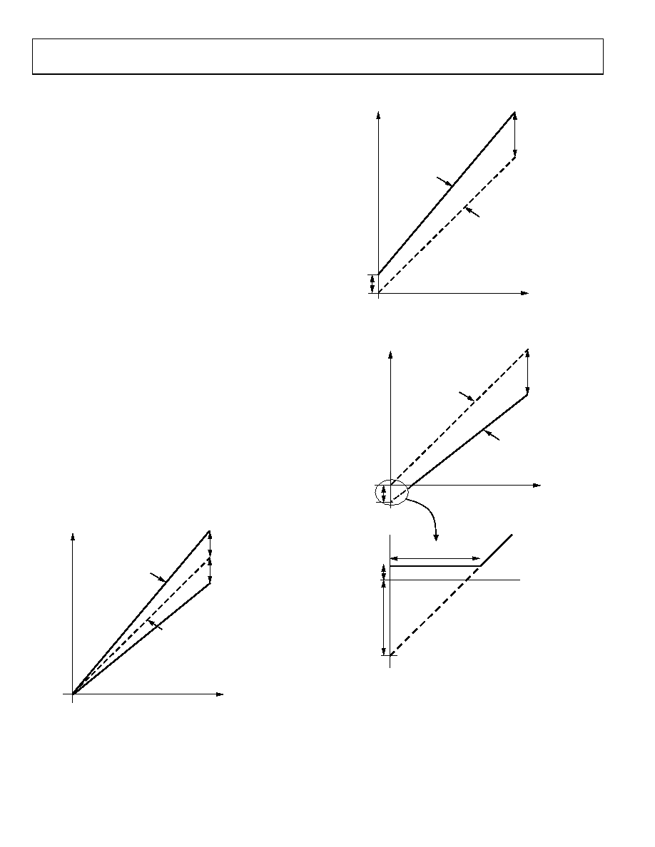
Gain Error
This is a measure of the span error of the DAC, including any
error in the gain of the buffer amplifier. It is the deviation in
slope of the actual DAC transfer characteristic from the ideal
and is expressed as a percentage of the full-scale range. This is
illustrated in Figure 11.
Offset Error
This is a measure of the offset error of the DAC and the output
amplifier. It is expressed as a percentage of the full-scale range.
If the offset voltage is positive, the output voltage still positive at
zero input code. This is shown in Figure 12. Because the DACs
operate from a single supply, a negative offset cannot appear at
the output of the buffer amplifier. Instead, there is a code close
to zero at which the amplifier output saturates (amplifier
footroom). Below this code there is a dead band over which the
output voltage does not change. This is illustrated in Figure 13.
OUTPUT
VOLTAGE
DAC CODE
POSITIVE
GAIN ERROR
NEGATIVE
GAIN ERROR
ACTUAL
IDEAL
03331-0-011
Figure 11. Gain Error
OUTPUT
VOLTAGE
DAC CODE
POSITIVE
OFFSET
GAIN ERROR
AND
OFFSET
ERROR
ACTUAL
IDEAL
03331-0-012
Figure 12. Positive Offset Error and Gain Error
AMPLIFIER
FOOTROOM
(~1mV)
NEGATIVE
OFFSET
OUTPUT
VOLTAGE
DAC CODE
GAIN ERROR
AND
OFFSET
ERROR
DEADBAND CODES
ACTUAL
IDEAL
NEGATIVE
OFFSET
03331-0-013
Figure 13. Negative Offset Error and Gain Error
相关PDF资料 |
PDF描述 |
|---|---|
| VI-23D-MY-B1 | CONVERTER MOD DC/DC 85V 50W |
| VE-B6L-MV-B1 | CONVERTER MOD DC/DC 28V 150W |
| VI-23B-MY-B1 | CONVERTER MOD DC/DC 95V 50W |
| VE-B6H-MV-B1 | CONVERTER MOD DC/DC 52V 150W |
| VI-234-MY-B1 | CONVERTER MOD DC/DC 48V 50W |
相关代理商/技术参数 |
参数描述 |
|---|---|
| AD5348BRU-REEL | 功能描述:IC DAC 12BIT OCTAL VOUT 38-TSSOP RoHS:否 类别:集成电路 (IC) >> 数据采集 - 数模转换器 系列:- 产品培训模块:Data Converter Fundamentals DAC Architectures 标准包装:750 系列:- 设置时间:7µs 位数:16 数据接口:并联 转换器数目:1 电压电源:双 ± 功率耗散(最大):100mW 工作温度:0°C ~ 70°C 安装类型:表面贴装 封装/外壳:28-LCC(J 形引线) 供应商设备封装:28-PLCC(11.51x11.51) 包装:带卷 (TR) 输出数目和类型:1 电压,单极;1 电压,双极 采样率(每秒):143k |
| AD5348BRU-REEL7 | 功能描述:IC DAC 12BIT OCTAL VOUT 38-TSSOP RoHS:否 类别:集成电路 (IC) >> 数据采集 - 数模转换器 系列:- 产品培训模块:Data Converter Fundamentals DAC Architectures 标准包装:750 系列:- 设置时间:7µs 位数:16 数据接口:并联 转换器数目:1 电压电源:双 ± 功率耗散(最大):100mW 工作温度:0°C ~ 70°C 安装类型:表面贴装 封装/外壳:28-LCC(J 形引线) 供应商设备封装:28-PLCC(11.51x11.51) 包装:带卷 (TR) 输出数目和类型:1 电压,单极;1 电压,双极 采样率(每秒):143k |
| AD5348BRUZ | 功能描述:IC DAC 12BIT OCTAL VOUT 38-TSSOP RoHS:是 类别:集成电路 (IC) >> 数据采集 - 数模转换器 系列:- 产品培训模块:Lead (SnPb) Finish for COTS Obsolescence Mitigation Program 标准包装:50 系列:- 设置时间:4µs 位数:12 数据接口:串行 转换器数目:2 电压电源:单电源 功率耗散(最大):- 工作温度:-40°C ~ 85°C 安装类型:表面贴装 封装/外壳:8-TSSOP,8-MSOP(0.118",3.00mm 宽) 供应商设备封装:8-uMAX 包装:管件 输出数目和类型:2 电压,单极 采样率(每秒):* 产品目录页面:1398 (CN2011-ZH PDF) |
| AD5348BRUZRUZ | 制造商:Analog Devices 功能描述:DAC,AD5348B 12bit 8us octal TSSOP |
| AD534J | 制造商:AD 制造商全称:Analog Devices 功能描述:Internally Trimmed Precision IC Multiplier |
发布紧急采购,3分钟左右您将得到回复。