- 您现在的位置:买卖IC网 > PDF目录373878 > AD534KD (ANALOG DEVICES INC) Dual 14-bit 125MSPS ADC with serialized LVDS output 48-VQFN -40 to 85 PDF资料下载
参数资料
| 型号: | AD534KD |
| 厂商: | ANALOG DEVICES INC |
| 元件分类: | 运动控制电子 |
| 英文描述: | Dual 14-bit 125MSPS ADC with serialized LVDS output 48-VQFN -40 to 85 |
| 中文描述: | ANALOG MULTIPLIER OR DIVIDER, 1 MHz BAND WIDTH, CDIP14 |
| 封装: | SIDE BRAZED, CERAMIC, TO-116, DIP-14 |
| 文件页数: | 3/12页 |
| 文件大小: | 159K |
| 代理商: | AD534KD |
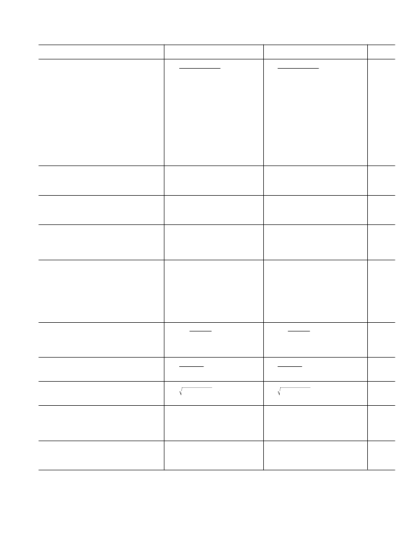
Model
AD534S
Typ
AD534T
Typ
Min
Max
Min
Max
Units
MULTIPLIER PERFORMANCE
Transfer Function
(
X
1
–
X
2
)(
Y
1
–
Y
2
)
10
V
+
Z
2
(
X
1
–
X
2
)(
Y
1
–
Y
2
)
10
V
+
Z
2
Total Error
1
(–10 V
≤
X, Y
≤
+10 V)
T
= min to max
Total Error vs. Temperature
Scale Factor Error
(SF = 10.000 V Nominal)
2
Temperature-Coefficient of
Scaling Voltage
Supply Rejection (
±
15 V
±
1 V)
Nonlinearity, X (X = 20 V p-p, Y = 10 V)
Nonlinearity, Y (Y = 20 V p-p, X = 10 V)
Feedthrough
3
, X (Y Nulled,
X = 20 V p-p 50 Hz)
Feedthrough
3
, Y (X Nulled,
Y = 20 V p-p 50 Hz)
Output Offset Voltage
Output Offset Voltage Drift
DYNAMICS
Small Signal BW (V
= 0.1 rms)
1% Amplitude Error (C
LOAD
= 1000 pF)
Slew Rate (V
20 p-p)
Settling Time (to 1%,
V
OUT
= 20 V)
NOISE
Noise Spectral-Density SF = 10 V
6
1.0
6
2.0
6
0.02
6
0.5
%
%
%/
°
C
±
1.0
6
0.01
±
0.25
±
0.1
%
±
0.02
±
0.01
±
0.4
±
0.2
6
0.005
%/
°
C
%
%
%
±
0.01
±
0.2
±
0.1
6
0.3
6
0.1
±
0.3
±
0.15
6
0.3
%
±
0.01
±
5
±
0.01
±
2
6
0.1
6
15
300
%
mV
μ
V/
°
C
±
30
500
1
50
20
2
1
50
20
2
MHz
kHz
V/
μ
s
μ
s
0.8
0.4
1.0
90
0.8
0.4
1.0
90
μ
V/
√
Hz
μ
V/
√
Hz
mV/rms
μ
V/rms
SF = 3V
4
Wideband Noise f = 10 Hz to 5 MHz
Wideband Noise
f = 10 Hz to 10 kHz
OUTPUT
Output Voltage Swing
Output Impedance (f
≤
1 kHz)
Output Short Circuit Current
(R
= 0, T
= min to max)
Amplifier Open Loop Gain (f = 50 Hz)
INPUT AMPLIFIERS (X, Y and Z)
5
Signal Voltage Range (Diff. or CM
Operating Diff.)
Offset Voltage X, Y
Offset Voltage Drift X, Y
Offset Voltage Z
Offset Voltage Drift Z
CMRR
Bias Current
Offset Current
Differential Resistance
DIVIDER PERFORMANCE
Transfer Function (X
1
> X
2
)
±
11
±
11
V
0.1
0.1
30
70
30
70
mA
dB
±
10
±
12
±
5
100
±
5
±
10
±
12
±
2
150
±
2
V
V
mV
μ
V/
°
C
mV
μ
V/
°
C
dB
μ
A
μ
A
M
6
20
6
10
6
30
500
6
15
300
60
80
0.8
0.1
10
70
90
0.8
0.1
10
2.0
2.0
10
V
(
Z
2
Z
1
)
(
X
1
X
2
)
+
Y
1
10
V
(
Z
2
Z
1
)
(
X
1
X
2
)
+
Y
1
Total Error
1
(X = 10 V, –10 V
≤
Z
≤
+10 V)
(X = 1 V, –1 V
≤
Z
≤
+1 V)
(0.1 V
≤
X
≤
10 V, –10 V
≤
Z
≤
10 V)
SQUARE PERFORMANCE
Transfer Function
±
0.75
±
2.0
±
2.5
±
0.35
±
1.0
±
1.0
%
%
%
(
X
1
X
2
)
2
10
V
+
Z
2
(
X
1
X
2
)
2
10
V
+
Z
2
Total Error (–10 V
≤
X
≤
10 V)
SQUARE-ROOTER PERFORMANCE
Transfer Function (Z
1
≤
Z
2
)
±
0.6
±
0.3
%
10
V
(
Z
2
Z
1
)
+
X
2
10
V
(
Z
2
Z
1
)
+
X
2
Total Error
1
(1 V
≤
Z
≤
10 V)
POWER SUPPLY SPECIFICATIONS
Supply Voltage
Rated Performance
Operating
Supply Current
Quiescent
PACKAGE OPTIONS
TO-100 (H-10A)
TO-116 (D-14)
E-20A
Chips
N
OTES
1
Figures given are percent of full scale,
±
10 V (i.e., 0.01% = 1 mV).
2
May be reduced down to 3 V using external resistor between –V
and SF.
3
Irreducible component due to nonlinearity: excludes effect of offsets.
4
Using external resistor adjusted to give SF = 3 V.
5
See Functional Block Diagram for definition of sections.
Specifications subject to change without notice.
±
1.0
±
0.5
%
±
15
±
15
V
V
±
8
6
22
±
8
6
22
4
6
4
6
mA
AD534SH
AD534SD
AD534SE
AD534S Chips
AD534TH
AD534TD
AD534T Chips
AD534
REV. B
–3–
S
pecifications shown in
boldface
are tested on all production units at final electrical
test. Results from those tests are used to calculate outgoing quality levels. All min and
max specifications are guaranteed, although only those shown in boldface are tested
on all production units.
相关PDF资料 |
PDF描述 |
|---|---|
| AD534KH | Dual 14-bit 125MSPS ADC with serialized LVDS output 48-VQFN -40 to 85 |
| AD534L | Dual 14-bit 125MSPS ADC with serialized LVDS output 48-VQFN -40 to 85 |
| AD534LD | Dual 14-bit 125MSPS ADC with serialized LVDS output 48-VQFN -40 to 85 |
| AD534LH | Internally Trimmed Precision IC Multiplier |
| AD534J | Internally Trimmed Precision IC Multiplier |
相关代理商/技术参数 |
参数描述 |
|---|---|
| AD534KD/+ | 制造商:未知厂家 制造商全称:未知厂家 功能描述:Analog Multiplier/Divider |
| AD534KDZ | 功能描述:IC PREC MULTIPLIER 14-CDIP RoHS:是 类别:集成电路 (IC) >> 线性 - 模拟乘法器,除法器 系列:- 标准包装:25 系列:HA 功能:模拟乘法器 位元/级数:四象限 封装/外壳:16-CDIP(0.300",7.62mm) 供应商设备封装:16-CDIP 侧面铜焊 包装:管件 |
| AD534KH | 功能描述:增效器/分频器 MULTIPLIER IC RoHS:否 制造商:Texas Instruments 产品:Multiplier 逻辑系列: 工作电源电压: 最大工作温度:+ 85 C 最小工作温度:- 40 C 安装风格:Through Hole 封装 / 箱体:PDIP-14 |
| AD534KH/+ | 制造商:Rochester Electronics LLC 功能描述:- Bulk |
| AD534KH+ | 制造商:AD 制造商全称:Analog Devices 功能描述:Internally Trimmed Precision IC Multiplier |
发布紧急采购,3分钟左右您将得到回复。