- 您现在的位置:买卖IC网 > PDF目录8564 > AD5361BCPZ-REEL7 (Analog Devices Inc)IC DAC 14BIT 16CH SERIAL 56LFCSP PDF资料下载
参数资料
| 型号: | AD5361BCPZ-REEL7 |
| 厂商: | Analog Devices Inc |
| 文件页数: | 19/29页 |
| 文件大小: | 0K |
| 描述: | IC DAC 14BIT 16CH SERIAL 56LFCSP |
| 产品培训模块: | Data Converter Fundamentals DAC Architectures |
| 标准包装: | 750 |
| 设置时间: | 20µs |
| 位数: | 14 |
| 数据接口: | 串行 |
| 转换器数目: | 16 |
| 电压电源: | 双 ± |
| 功率耗散(最大): | 245mW |
| 工作温度: | -40°C ~ 85°C |
| 安装类型: | 表面贴装 |
| 封装/外壳: | 56-VFQFN 裸露焊盘,CSP |
| 供应商设备封装: | 56-LFCSP-VQ(8x8) |
| 包装: | 带卷 (TR) |
| 输出数目和类型: | 16 电压,单极;16 电压,双极 |
| 采样率(每秒): | * |
| 配用: | EVAL-AD5361EBZ-ND - BOARD EVAL FOR AD5361 |
第1页第2页第3页第4页第5页第6页第7页第8页第9页第10页第11页第12页第13页第14页第15页第16页第17页第18页当前第19页第20页第21页第22页第23页第24页第25页第26页第27页第28页第29页
AD5360/AD5361
Rev. A | Page 25 of 28
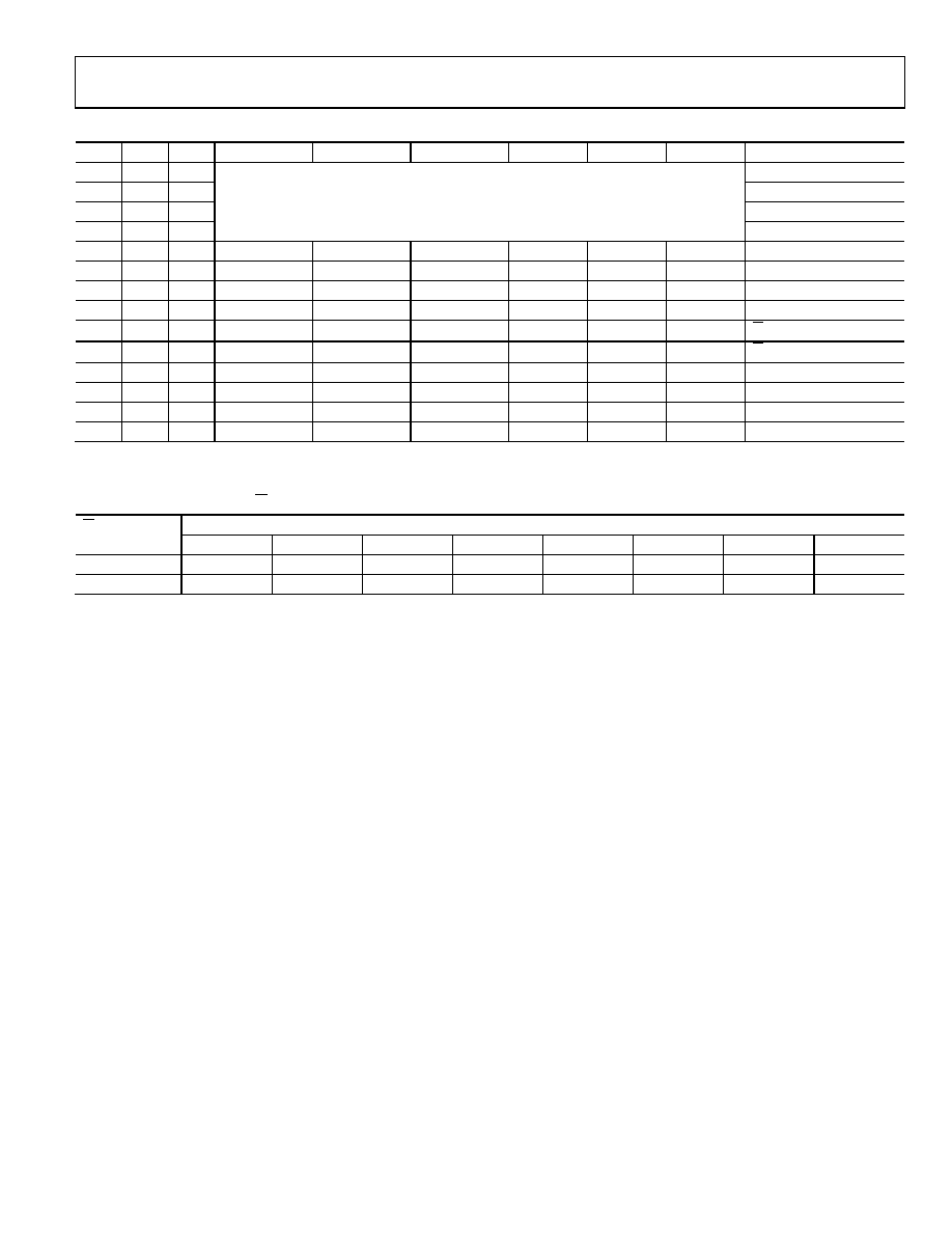
Table 16. Address Codes for Data Readback1
F15
F14
F13
F12
F11
F10
F9
F8
F7
Register Read
0
Bit F12 to Bit F7 select channel to be read back,
Channel 0 = 001000 to Channel 15 = 010111
X1A Register
0
1
X1B Register
0
1
0
C Register
0
1
M Register
1
0
1
Control Register
1
0
1
0
OFS0 Data Register
1
0
1
OFS1 Data Register
1
0
1
0
Reserved
1
0
1
0
A/B Select Register 0
1
0
1
A/B Select Register 1
1
0
1
0
Reserved
1
0
1
0
1
Reserved
1
0
1
0
1
0
Reserved
1
0
1
0
1
GPIO Read (Data in F0)2
1 F6 to F0 are don’t cares for the data readback function.
2 F6 to F0 should be 0 for GPIO read.
Table 17. DACs Selected by A/B Select Registers
A/B Select
Register
F7
F6
F5
F4
F3
F2
F1
F0
0
DAC7
DAC6
DAC5
DAC4
DAC3
DAC2
DAC1
DAC0
1
DAC15
DAC14
DAC13
DAC12
DAC11
DAC10
DAC9
DAC8
1 If the bit is 0, Register X2A is selected. If the bit is 1, Register X2B is selected.
POWER SUPPLY DECOUPLING
In any circuit where accuracy is important, careful considera-
tion of the power supply and ground return layout helps to
ensure the rated performance. The printed circuit board on
which the AD5360/AD5361 are mounted should be designed so
that the analog and digital sections are separated and confined
to certain areas of the board. If the AD5360/AD5361 are in a
system where multiple devices require an AGND-to-DGND
connection, the connection should be made at one point only.
The star ground point should be established as close as possible
to the device. For supplies with multiple pins (VSS, VDD, DVCC),
it is recommended to tie these pins together and to decouple
each supply once.
The AD5360/AD5361 should have ample supply decoupling of
10 μF in parallel with 0.1 μF on each supply located as close to
the package as possible, ideally right up against the device. The
10 μF capacitors are the tantalum bead type. The 0.1 μF capaci-
tor should have low effective series resistance (ESR) and effective
series inductance (ESI), such as the common ceramic types that
provide a low impedance path to ground at high frequencies, to
handle transient currents due to internal logic switching.
Digital lines running under the device should be avoided
because these couple noise onto the device. The analog ground
plane should be allowed to run under the AD5360/AD5361 to
avoid noise coupling. The power supply lines of the AD5360/
AD5361 should use as large a trace as possible to provide low
impedance paths and reduce the effects of glitches on the power
supply line. Fast switching digital signals should be shielded
with digital ground to avoid radiating noise to other parts of the
board and should never be run near the reference inputs. It is
essential to minimize noise on all VREFx lines.
Avoid crossover of digital and analog signals. Traces on
opposite sides of the board should run at right angles to each
other. This reduces the effects of feedthrough through the
board. A microstrip technique is by far the best, but this is not
always possible with a double-sided board. In this technique,
the component side of the board is dedicated to the ground
plane, while signal traces are placed on the solder side.
As is the case for all thin packages, care must be taken to avoid
flexing the package and to avoid a point load on the surface of
this package during the assembly process.
POWER SUPPLY SEQUENCING
When the supplies are connected to the AD5360/AD5361, it is
important that the AGND and DGND pins be connected to the
relevant ground plane before the positive or negative supplies
are applied. In most applications, this is not an issue because the
ground pins for the power supplies are connected to the ground
pins of the AD5360/AD5361 via ground planes. Where the
AD5360/AD5361 are used in a hot-swap card, care should be
taken to ensure that the ground pins are connected to the
supply grounds before the positive or negative supplies are
connected. This is required to prevent currents from flowing in
directions other than toward an analog or digital ground.
相关PDF资料 |
PDF描述 |
|---|---|
| AD7537LPZ | IC DAC 12BIT DUAL MULT 28PLCC |
| VI-2ND-IV | CONVERTER MOD DC/DC 85V 150W |
| VI-261-IV | CONVERTER MOD DC/DC 12V 150W |
| VI-B3R-MU-S | CONVERTER MOD DC/DC 7.5V 200W |
| VI-BW0-MX-S | CONVERTER MOD DC/DC 5V 75W |
相关代理商/技术参数 |
参数描述 |
|---|---|
| AD5361BCPZ-REEL71 | 制造商:AD 制造商全称:Analog Devices 功能描述:16-Channel, 16-/14-Bit, Serial Input, Voltage-Output DAC |
| AD5361BSTZ | 功能描述:IC DAC 14BIT 16CH SERIAL 56LQFP RoHS:是 类别:集成电路 (IC) >> 数据采集 - 数模转换器 系列:- 产品培训模块:Lead (SnPb) Finish for COTS Obsolescence Mitigation Program 标准包装:1,000 系列:- 设置时间:1µs 位数:8 数据接口:串行 转换器数目:8 电压电源:双 ± 功率耗散(最大):941mW 工作温度:0°C ~ 70°C 安装类型:表面贴装 封装/外壳:24-SOIC(0.295",7.50mm 宽) 供应商设备封装:24-SOIC W 包装:带卷 (TR) 输出数目和类型:8 电压,单极 采样率(每秒):* |
| AD5361BSTZ1 | 制造商:AD 制造商全称:Analog Devices 功能描述:16-Channel, 16-/14-Bit, Serial Input, Voltage-Output DAC |
| AD5361BSTZ-REEL | 功能描述:IC DAC 14BIT 16CH SERIAL 52-LQFP RoHS:是 类别:集成电路 (IC) >> 数据采集 - 数模转换器 系列:- 产品培训模块:Lead (SnPb) Finish for COTS Obsolescence Mitigation Program 标准包装:1,000 系列:- 设置时间:1µs 位数:8 数据接口:串行 转换器数目:8 电压电源:双 ± 功率耗散(最大):941mW 工作温度:0°C ~ 70°C 安装类型:表面贴装 封装/外壳:24-SOIC(0.295",7.50mm 宽) 供应商设备封装:24-SOIC W 包装:带卷 (TR) 输出数目和类型:8 电压,单极 采样率(每秒):* |
| AD5361BSTZ-REEL1 | 制造商:AD 制造商全称:Analog Devices 功能描述:16-Channel, 16-/14-Bit, Serial Input, Voltage-Output DAC |
发布紧急采购,3分钟左右您将得到回复。