参数资料
| 型号: | AD5363BSTZ |
| 厂商: | Analog Devices Inc |
| 文件页数: | 28/29页 |
| 文件大小: | 0K |
| 描述: | IC DAC 14BIT 8CH SERIAL 52-LQFP |
| 产品培训模块: | Data Converter Fundamentals DAC Architectures |
| 标准包装: | 1 |
| 设置时间: | 20µs |
| 位数: | 14 |
| 数据接口: | 串行 |
| 转换器数目: | 8 |
| 电压电源: | 双 ± |
| 功率耗散(最大): | 209mW |
| 工作温度: | -40°C ~ 85°C |
| 安装类型: | 表面贴装 |
| 封装/外壳: | 52-LQFP |
| 供应商设备封装: | 52-LQFP(10x10) |
| 包装: | 托盘 |
| 输出数目和类型: | 8 电压,单极;8 电压,双极 |
| 采样率(每秒): | * |
| 配用: | EVAL-AD5363EBZ-ND - BOARD EVALUATION FOR AD5363 |
第1页第2页第3页第4页第5页第6页第7页第8页第9页第10页第11页第12页第13页第14页第15页第16页第17页第18页第19页第20页第21页第22页第23页第24页第25页第26页第27页当前第28页第29页
AD5362/AD5363
Rev. A | Page 7 of
28
TIMING CHARACTERISTICS
DVCC = 2.5 V to 5.5 V; VDD = 9 V to 16.5 V; VSS = 16.5 V to 8 V; VREF = 5 V; AGND = DGND = SIGGND = 0 V; CL = 200 pF to GND;
RL = open circuit; gain (M), offset (C), and DAC offset registers at default values; all specifications TMIN to TMAX, unless otherwise noted.
Table 4. SPI Interface
Limit at TMIN, TMAX
Unit
Description
t1
20
ns min
SCLK cycle time
t2
8
ns min
SCLK high time
t3
8
ns min
SCLK low time
t4
11
ns min
SYNC falling edge to SCLK falling edge setup time
t5
20
ns min
Minimum SYNC high time
t6
10
ns min
24th SCLK falling edge to SYNC rising edge
t7
5
ns min
Data setup time
t8
5
ns min
Data hold time
42
ns max
SYNC rising edge to BUSY falling edge
t10
1/1.5
μs typ/μs max
BUSY pulse width low (single-channel update); see Table 9
t11
600
ns max
Single-channel update cycle time
t12
20
ns min
SYNC rising edge to LDAC falling edge
t13
10
ns min
LDAC pulse width low
t14
3
μs max
BUSY rising edge to DAC output response time
t15
0
ns min
BUSY rising edge to LDAC falling edge
t16
3
μs max
LDAC falling edge to DAC output response time
t17
20/30
μs typ/μs max
DAC output settling time
t18
140
ns max
CLR/RESET pulse activation time
t19
30
ns min
RESET pulse width low
t20
400
μs max
RESET time indicated by BUSY low
t21
270
ns min
Minimum SYNC high time in readback mode
25
ns max
SCLK rising edge to SDO valid
t23
80
ns max
RESET rising edge to BUSY falling edge
1 Guaranteed by design and characterization
; not production tested.
2 All input signals are specified with tR = tF = 2 ns (10% to 90% of DVCC) and timed from a voltage level of 1.2 V.
3 See Figure 4 and Figure 5.
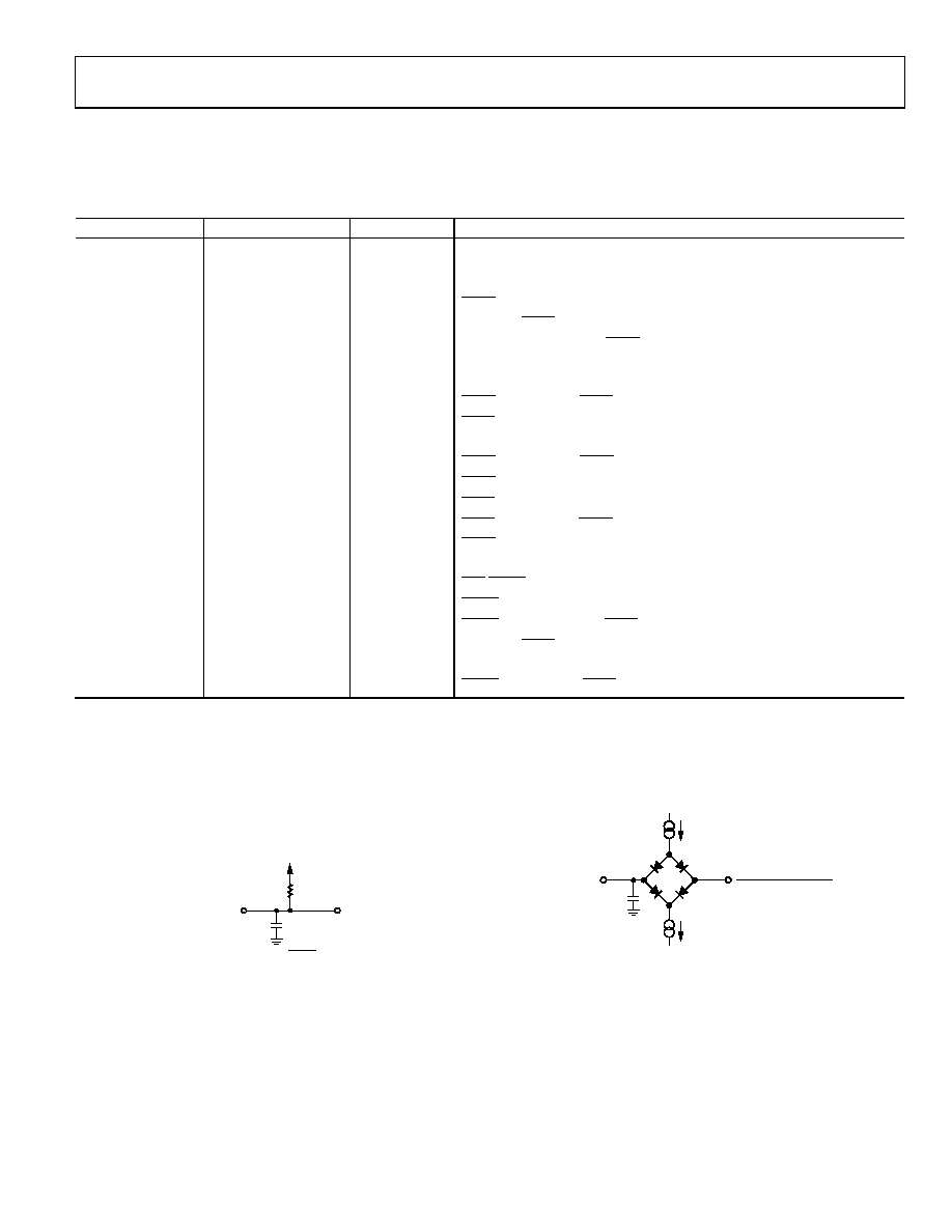
4 t9 is measured with the load circuit shown in Figure 2.
5 t22 is measured with the load circuit shown in Figure 3.
TO
OUTPUT
PIN
CL
50pF
RL
2.2k
VOL
DVCC
05
76
2-
00
2
VOH (MIN) – VOL (MAX)
2
200A
IOL
200A
IOH
TO OUTPUT
PIN
CL
50pF
0
57
62
-00
3
Figure 2. Load Circuit for BUSY Timing Diagram
Figure 3. Load Circuit for SDO Timing Diagram
相关PDF资料 |
PDF描述 |
|---|---|
| AD5370BSTZ | IC DAC 16BIT 40CH SERIAL 64-LQFP |
| AD5373BSTZ | IC DAC 14BIT 32CH SER 64-LQFP |
| AD5378ABC | IC DAC 14BIT 32CHAN 108CSPBGA |
| AD5379ABC | IC DAC 14BIT 40CH 108-CSPBGA |
| AD5380BSTZ-3 | IC DAC 14BIT 40CHAN 3V 100LQFP |
相关代理商/技术参数 |
参数描述 |
|---|---|
| AD5363BSTZ-REEL | 功能描述:IC DAC 14BIT 8CH SERIAL 52-LQFP RoHS:是 类别:集成电路 (IC) >> 数据采集 - 数模转换器 系列:- 产品培训模块:Data Converter Fundamentals DAC Architectures 标准包装:750 系列:- 设置时间:7µs 位数:16 数据接口:并联 转换器数目:1 电压电源:双 ± 功率耗散(最大):100mW 工作温度:0°C ~ 70°C 安装类型:表面贴装 封装/外壳:28-LCC(J 形引线) 供应商设备封装:28-PLCC(11.51x11.51) 包装:带卷 (TR) 输出数目和类型:1 电压,单极;1 电压,双极 采样率(每秒):143k |
| AD5365D/BIN/883B | 制造商:Analog Devices 功能描述:- Rail/Tube |
| AD536A | 制造商:AD 制造商全称:Analog Devices 功能描述:Integrated Circuit True RMS-to-DC Converter |
| AD536AJC/D | 制造商:未知厂家 制造商全称:未知厂家 功能描述:RMS-to-DC Converter |
| AD536AJCHIPS | 制造商:AD 制造商全称:Analog Devices 功能描述:Integrated Circuit True RMS-to-DC Converter |
发布紧急采购,3分钟左右您将得到回复。