- 您现在的位置:买卖IC网 > PDF目录22188 > AD536ASD (Analog Devices Inc)IC TRUE RMS/DC CONV 14-CDIP PDF资料下载
参数资料
| 型号: | AD536ASD |
| 厂商: | Analog Devices Inc |
| 文件页数: | 1/17页 |
| 文件大小: | 552K |
| 描述: | IC TRUE RMS/DC CONV 14-CDIP |
| 产品培训模块: | Introduction to Analog RMS-to-DC Technology: Converters and Applications |
| 标准包装: | 1 |
| 电流 - 电源: | 1.2mA |
| 电源电压: | 5.0V ~ 36V,±3.0V ~ 18V |
| 安装类型: | 通孔 |
| 封装/外壳: | 14-CDIP(0.300",7.62mm) |
| 供应商设备封装: | 14-CDIP |
| 包装: | 管件 |
| 产品目录页面: | 786 (CN2011-ZH PDF) |
Integrated Circuit
True RMS-to-DC Converter
Data Sheet
AD536A
Rev. E
Information furnished by Analog Devices is believed to be accurate and reliable. However, no
responsibility is assumed by Analog Devices for its use, nor for any infringements of patents or other
rights of third parties that may result from its use. Specifications subject to change without notice. No
license is granted by implication or otherwise under any patent or patent rights of Analog Devices.
Tr mrk n r i r r mrk r h r r fh irr iv wn r
One Technology Way, P.O. Box 9106, Norwood, MA 02062-9106, U.S.A.
Tel: 781.329.4700
www.analog.com
F x 7 14 1 11 ? 7 2 12An l vi In Allri h r rv
FEATURES
True rms-to-dc conversion
Laser trimmed to high accuracy
?.2% maximum error (AD536AK)
?.5% maximum error (AD536AJ)
Wide response capability
Computes rms of ac and dc signals
450 kHz bandwidth: V rms > 100 mV
2 MHz bandwidth: V rms > 1 V
Signal crest factor of 7 for 1% error
dB output with 60 dB range
Low power: 1.2 mA quiescent current
Single- or dual-supply operation
Monolithic integrated circuit
55癈 to +125癈 operation (AD536AS)
GENERAL DESCRIPTION
The AD536A is a complete monolithic integrated circuit that
performs true rms-to-dc conversion. It offers performance
comparable or superior to that of hybrid or modular units costing
much more. The AD536A directly computes the true rms value of
any complex input waveform containing ac and dc components.
A crest factor compensation scheme allows measurements with 1%
error at crest factors up to 7. The wide bandwidth of the device
extends the measurement capability to 300 kHz with less than 3 dB
errors for signal levels greater than 100 mV.
An important feature of the AD536A, not previously available
in rms converters, is an auxiliary dB output pin. The logarithm
of the rms output signal is brought out to a separate pin to allow
the dB conversion, with a useful dynamic range of 60 dB. Using
an externally supplied reference current, the 0 dB level can be
conveniently set to correspond to any input level from 0.1 V to
2 V rms.
The AD536A is laser trimmed to minimize input and output offset
voltage, to optimize positive and negative waveform symmetry
(dc reversal error), and to provide full-scale accuracy at 7 V rms.
As a result, no external trims are required to achieve the rated
unit accuracy.
The input and output pins are fully protected. The input circuitry
can take overload voltages well beyond the supply levels. Loss of
supply voltage with the input connected to external circuitry does
not cause the device to fail. The output is short-circuit protected.
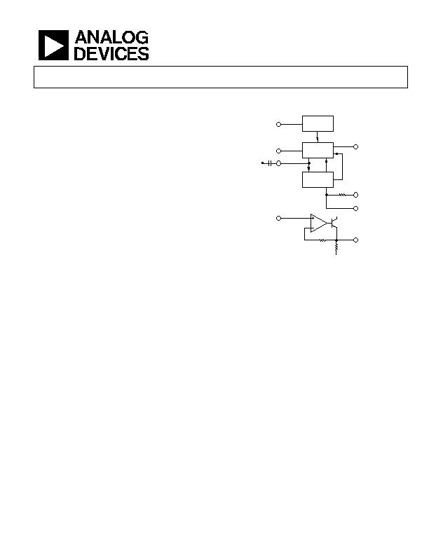
FUNCTIONAL BLOCK DIAGRAM
dB
UFFER IN
V
IN
25k&
80k&
25k&
C
AV
V
S
V
S
COM
AD536A
R
L
I
OUT
BUFFER
OUT
CURRENT
MIRROR
SQUARER/
DIVIDER
ABSOLUTE
VALUE
+
BUF
Figure 1.
The AD536A is available in two accuracy grades (J and K) for
commercial temperature range (0癈 to 70癈) applications, and
one grade (S) rated for the 55癈 to +125癈 extended range.
The AD536AK offers a maximum total error of ? mV ?0.2%
of reading, while the AD536AJ and AD536AS have maximum
errors of ? mV ?0.5% of reading. All three versions are available
in a hermetically sealed 14-lead DIP or a 10-pin TO-100 metal
header package. The AD536AS is also available in a 20-terminal
leadless hermetically sealed ceramic chip carrier.
The AD536A computes the true root-mean-square level of a
complex ac (or ac plus dc) input signal and provides an equiva-
lent dc output level. The true rms value of a waveform is a more
useful quantity than the average rectified value because it relates
directly to the power of the signal. The rms value of a statistical
signal also relates to its standard deviation.
An external capacitor is required to perform measurements to the
fully specified accuracy. The value of this capacitor determines the
low frequency ac accuracy, ripple amplitude, and settling time.
The AD536A operates equally well from split supplies or a
single supply with total supply levels from 5 V to 36 V. With
1 mA quiescent supply current, the device is well suited for a
wide variety of remote controllers and battery-powered
instruments.
相关PDF资料 |
PDF描述 |
|---|---|
| AD536ASH | IC TRUE RMS/DC CONV TO-100-10 |
| RAC30-12SA | CONV AC/DC 2A 6.5-18VIN 3.0-5.5V |
| WSU135-0880-R | POWER SUPPLY 100-240V 880MA |
| NCP4680DMX23TCG | IC REG LDO 2.3V .15A 4XDFN |
| WSU050-1500 | POWER SUPPLY 100-240V 1500MA |
相关代理商/技术参数 |
参数描述 |
|---|---|
| AD536ASD/883B | 功能描述:直流/直流开关转换器 RMS/DC CONVERTER IC RoHS:否 制造商:STMicroelectronics 最大输入电压:4.5 V 开关频率:1.5 MHz 输出电压:4.6 V 输出电流:250 mA 输出端数量:2 最大工作温度:+ 85 C 安装风格:SMD/SMT |
| AD536ASD883B | 制造商:ANALOG DEV 功能描述:DIP-14PIN GOLD |
| AD536ASE | 制造商:Rochester Electronics LLC 功能描述: 制造商:Rochester Electronics LLC 功能描述:- Bulk 制造商:Analog Devices 功能描述: |
| AD536ASE/883B | 功能描述:直流/直流开关转换器 RMS/DC CONVERTER IC RoHS:否 制造商:STMicroelectronics 最大输入电压:4.5 V 开关频率:1.5 MHz 输出电压:4.6 V 输出电流:250 mA 输出端数量:2 最大工作温度:+ 85 C 安装风格:SMD/SMT |
| AD536ASH | 功能描述:IC TRUE RMS/DC CONV TO-100-10 RoHS:否 类别:集成电路 (IC) >> PMIC - RMS 至 DC 转换器 系列:- 标准包装:46 系列:- 电流 - 电源:1.2mA 电源电压:±18 V,36 V 安装类型:表面贴装 封装/外壳:16-SOIC(0.295",7.50mm 宽) 供应商设备封装:16-SOIC W 包装:管件 |
发布紧急采购,3分钟左右您将得到回复。