- 您现在的位置:买卖IC网 > PDF目录22164 > AD537SH (Analog Devices Inc)IC V/F CONV TO100-10 PDF资料下载
参数资料
| 型号: | AD537SH |
| 厂商: | Analog Devices Inc |
| 文件页数: | 6/8页 |
| 文件大小: | 683K |
| 描述: | IC V/F CONV TO100-10 |
| 标准包装: | 1 |
| 类型: | 电压至频率 |
| 频率 - 最大: | 100kHz |
| 全量程: | ±30ppm/°C |
| 线性: | ±0.05% |
| 安装类型: | 通孔 |
| 封装/外壳: | TO-100-10 金属罐 |
| 供应商设备封装: | TO-100-10 |
| 包装: | 管件 |
AD537
REV. C
6
F-V CONVERTERS
The AD537 can be used as a high linearity VCO in a phase-
locked loop to accomplish frequency-to-voltage conversion. By
operating the loop without a low-pass filter in the feedback path
(first-order system), it can lock to any frequency from zero to an
upper limit determined by the design, responding in three or
four cycles to a step change of input frequency. In practice, the
overall response time is determined by the characteristics of the
averaging filter which follows the PLL.
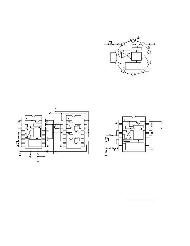
Figure 7 shows a connection using a low power TTL quad
open-collector nand gate which serves as the phase comparator.
The input signal should be a pulse train or square wave with
characteristics similar to TTL or 5-volt CMOS outputs. Any
duty cycle is acceptable, but the minimum pulse width is 40祍.
The output voltage is one volt for a 10kHz input frequency.
The output as shown here is at a fairly high impedance level; for
many situations an additional buffer may be required.
Trimming is similar to V-F application trimming. First set the
V
OS
trimmer to mid-scale. Apply a 10kHz input frequency and
trim the 2k& potentiometer for 1.00 volts out. Then apply a
10Hz waveform and trim the V
OS
for 1mV out. Finally, retrim
the full-scale output at 10kHz. Other frequency scales can be
obtained by appropriate scaling of timing components.
1
2
14
13
5
6
7
10
9
8
3
4
12
11
AD537
DRIVER
PRECISION
VOLTAGE
REFERENCE
CURR
-TO-
FREQ
CONV
BUF
20k
V
OS
f
IN
(0-10kHz)
2k
10k
0.001礔
1N4148
0.005礔
3.9k
120k
OUTPUT
1V F.S.
0.33礔
10k
10k
74LO3
+5V
10k
9.09k
Figure 7. 10kHz F-V Converter
TEMPERATURE-TO-FREQUENCY CONVERSION
The linear temperature-proportional output of the AD537 can
be used as shown in these applications to perform various direct
temperature-to-frequency conversion functions; it can also be
used with other external connections in a temperature sensing
or compensation scheme. If the sensor output is used externally,
it should be buffered through an op amp since loading that
point will cause significant error in the sensor output as well as
in the main V-F converter circuitry.
An absolute temperature (Kelvin)-to-frequency converter is very
easily accomplished, as shown in Figure 8. The 1mV per K out-
put serves as the input to the buffer amplifier, which then scales
the oscillator drive current to a nominal 298礎 at +25癈
(298K). Use of a 1000pF capacitor results in a corresponding
frequency of 2.98kHz. Setting the single 2 k& trimmer for the
correct frequency at a well-defined temperature near +25癈 will
normally result in an accuracy of ?癈 from 55癈 to +125癈
(using an AD537S). An NPO ceramic capacitor is recom-
mended to minimize nonlinearity due to capacitance drift.
DRIVER
CURR-
TO-FREQ
CONV
PRECISION
VOLTAGE
REFERENCE
V
T
V
R
AD537
+V
V
TEMP
V
REF
LOGIC
GND
+V
S
V
S
(CONNECTED TO CASE)
10
9
8
7
6
5
4
3
2
1
9.1k&
10k&
f = 10Hz/K
1000pF
2k&
BUF
Figure 8. Absolute Temperature to Frequency Converter
OFFSET TEMPERATURE SCALES
Many other temperature scales can be set up by offsetting the
temperature output with the voltage reference output. Such a
scheme is shown by the Celsius-to-frequency converter in
Figure 9. Corresponding component values for a Fahrenheit-to-
frequency converter which give 10Hz/癋 are given in parentheses.
1
2
14
13
5
6
7
10
9
8
3
4
12
11
AD537
10k
f
OUT
10Hz/?/SPAN>C
(10Hz/?/SPAN>F)
+5V
2.74k
(4.02k)
500&
3900 pF
(1500pF)
2k
6.04k
(10k)
49&
(205&)
BUF
DRIVER
CURR-
TO-FREQ
CONV
PRECISION
VOLTAGE
REFERENCE
V
T
V
R
Figure 9. Offset Temperature Scale Converters Centigrade
and (Fahrenheit) to Frequency
A simple calibration procedure which will provide ?癈 accu-
racy requires substitution of a 7.27k resistor for the series com-
bination of the 6.04k with the 2k trimmer; then simply set the
500& trimmer to give 250Hz at +25癈.
High accuracy calibration procedure:
1. Measure room temperature in K.
2. Measure temperature output at Pin 6 at that temperature.
3. Calculate offset adjustment as follows:
Offset Voltage (mV) =
V
TEMP
(Pin 6) (mV)
Room temp (K)
?73.2
4. Temporarily disconnect 49& resistor (or 500& pot) and
trim 2k& pot to give the offset voltage at the indicated node.
Reconnect 49& resistor.
5. Adjust slope trimmer to give proper frequency at room tem-
perature (+25癈 = 250Hz).
Adjustment for 癋 or any other scale is analogous.
相关PDF资料 |
PDF描述 |
|---|---|
| IDT71256SA15Y | IC SRAM 256KBIT 15NS 28SOJ |
| RSM30DTBD-S189 | CONN EDGECARD 60POS R/A .156 SLD |
| V28A3V3C150BF2 | CONVERTER MOD DC/DC 3.3V 150W |
| AD650KNZ | IC CONVERTER V-F/F-V 14DIP |
| RBC13DRYN | CONN EDGECARD 26POS .100 EXTEND |
相关代理商/技术参数 |
参数描述 |
|---|---|
| AD537SH/883B | 功能描述:电压频率转换及频率电压转换 IC MONO V/F CONVERTER IC RoHS:否 制造商:Texas Instruments 全标度频率:4000 KHz 线性误差:+/- 1 % FSR 电源电压-最大: 电源电压-最小: 最大工作温度:+ 85 C 最小工作温度:- 25 C 安装风格:Through Hole 封装 / 箱体:PDIP-14 封装:Tube |
| AD5380BST-3 | 制造商:Analog Devices 功能描述:DAC 40-CH Resistor-String 14-bit 100-Pin LQFP 制造商:Rochester Electronics LLC 功能描述:32/40-CHANNEL 3V/5V SINGLE SUPPLY 12/14-BIT VOUT DAC - Bulk |
| AD5380BST-3-REEL | 制造商:Analog Devices 功能描述:DAC 40-CH Resistor-String 14-bit 100-Pin LQFP T/R |
| AD5380BST-5 | 制造商:Analog Devices 功能描述:DAC 40-CH Resistor-String 14-bit 100-Pin LQFP 制造商:Rochester Electronics LLC 功能描述:40-CHN 5V SINGLE SUPPLY 14-BIT VOUT I.C. - Bulk |
| AD5380BST-5-REEL | 制造商:Analog Devices 功能描述:DAC 40-CH Resistor-String 14-bit 100-Pin LQFP T/R |
发布紧急采购,3分钟左右您将得到回复。