参数资料
| 型号: | AD5390BCPZ-5 |
| 厂商: | Analog Devices Inc |
| 文件页数: | 29/44页 |
| 文件大小: | 0K |
| 描述: | IC DAC 14BIT 16CHAN 5V 64LFCSP |
| 产品培训模块: | Data Converter Fundamentals DAC Architectures |
| 产品变化通告: | AD5390/1/2 Redesign Change 16/May/2012 |
| 设计资源: | 8 to 16 Channels of Programmable Voltage with Excellent Temperature Drift Performance Using AD5390/1/2 (CN0029) AD5390/91/92 Channel Monitor Function (CN0030) |
| 标准包装: | 1 |
| 设置时间: | 8µs |
| 位数: | 14 |
| 数据接口: | I²C,串行 |
| 转换器数目: | 16 |
| 电压电源: | 单电源 |
| 功率耗散(最大): | 35mW |
| 工作温度: | -40°C ~ 85°C |
| 安装类型: | 表面贴装 |
| 封装/外壳: | 64-VFQFN 裸露焊盘,CSP |
| 供应商设备封装: | 64-LFCSP-VQ(9x9) |
| 包装: | 托盘 |
| 输出数目和类型: | 16 电压,单极 |
| 采样率(每秒): | 125k |
| 配用: | EVAL-AD5390EBZ-ND - BOARD EVALUATION FOR AD5390 |
第1页第2页第3页第4页第5页第6页第7页第8页第9页第10页第11页第12页第13页第14页第15页第16页第17页第18页第19页第20页第21页第22页第23页第24页第25页第26页第27页第28页当前第29页第30页第31页第32页第33页第34页第35页第36页第37页第38页第39页第40页第41页第42页第43页第44页
Data Sheet
AD5390/AD5391/AD5392
Rev. E | Page 35 of 44
HARDWARE FUNCTIONS
RESET FUNCTION
Bringing the RESET line low resets the contents of all internal
registers to their power-on reset state. RESET is a negative edge-
sensitive input. The default corresponds to m at full scale and
c at zero scale. The contents of all DAC registers are cleared by
setting the outputs to 0 V. This sequence takes 270 s maximum.
The falling edge of RESET initiates the reset process. BUSY goes
low for the duration, returning high when RESET is complete.
While BUSY is low, all interfaces are disabled and all LDAC
pulses are ignored. When BUSY returns high, the part resumes
normal operation, and the status of the RESET pin is ignored
until the next falling edge is detected.
ASYNCHRONOUS CLEAR FUNCTION
CLR is negative-edge-triggered and BUSY goes low for the
duration of the CLR execution. Bringing the CLR line low
clears the contents of the DAC registers to the data contained in
the user-configurable CLR register and sets the analog outputs
accordingly. This function can be used in system calibration
to load zero scale and full scale to all channels together. The
execution time for a CLR is 20 s on the AD5390/AD5391 and
15 s on the AD5392.
BUSY AND LDAC FUNCTIONS
BUSY is a digital CMOS output indicating the status of the
AD539x devices. BUSY goes low during internal calculations
of x2 data. If LDAC is taken low while BUSY is low, this event
is stored. The user can hold the LDAC input permanently low
and, in this case, the DAC outputs update immediately
after BUSY goes high. BUSY also goes low during a power-on
reset and when a falling edge is detected on the RESET pin.
During this time, all interfaces are disabled and any events
on LDAC
are ignored.
The AD539x products contain an extra feature whereby a DAC
register is not updated unless its x2 register has been written
to since the last time LDAC was brought low. Normally,
when LDAC is brought low, the DAC registers are filled with
the contents of the x2 registers. However, these devices update
the DAC register only if the x2 data has changed, thereby
removing unnecessary digital crosstalk.
POWER-ON RESET
The AD539x products contain a power-on reset generator
and state machine. The power-on reset resets all registers to a
predefined state, and the analog outputs are configured as high
impedance outputs. The BUSY pin goes low during the power-
on reset sequence, preventing data writes to the device.
POWER-DOWN
The AD539x products contain a global power-down feature that
puts all channels into a low power mode, reducing the analog
power consumption to 1 A maximum and the digital power
consumption to 20 A maximum. In power-down mode, the
output amplifier can be configured as a high impedance output
or to provide a 100 k load to ground. The contents of all
internal registers are retained in power-down mode. When
exiting power-down, the settling time of the amplifier elapses
before the outputs settle to their correct value.
MICROPROCESSOR INTERFACING
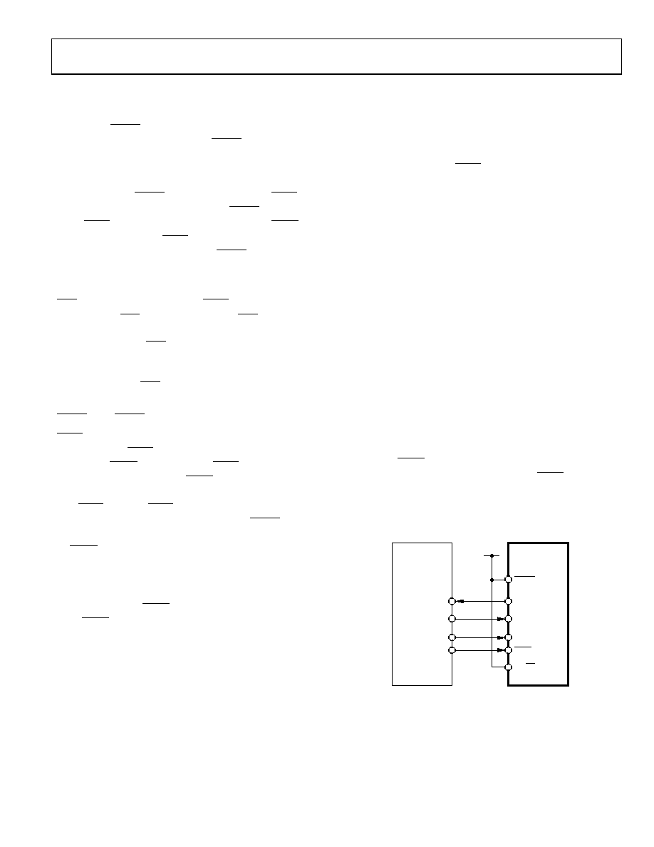
AD539x to MC68HC11
The serial peripheral interface (SPI) on the MC68HC11 is
configured for master mode (MSTR = 1), clock polarity bit
(CPOL) = 0, and the clock phase bit (CPHA) = 1. The SPI is
configured by writing to the SPI control register (SPCR)—see
the 68HC11 User Manual. SCK of the MC68HC11 drives the
SCLK of the AD539x, the MOSI output drives the serial data
line (DIN) of the AD539x, and the MISO input is driven from
DOUT. The SYNC signal is derived from a port line (PC7). When
data is being transmitted to the AD539x, the SYNC line is taken
low (PC7). Data appearing on the MOSI output is valid on the
falling edge of SCK. Serial data from the MC8HC11 is trans-
mitted in 8-bit bytes with only eight falling clock edges
occurring in the transmit cycle.
DVDD
MC68HC11
SDO
DIN
AD539x
SCLK
RESET
SYNC
MISO
MOSI
SCK
PC7
SPI/I2C
03773-
026
Figure 37. AD539x-MC68HC11 Interface
相关PDF资料 |
PDF描述 |
|---|---|
| AD5398ABCBZ-REEL | IC DAC 10BIT CURRENT-SINK 9WLCSP |
| AD5405YCPZ-REEL7 | IC DAC DUAL 12BIT MULT 40LFCSP |
| AD5415YRU | IC DAC DUAL 12BIT MULT 24-TSSOP |
| AD5421CREZ | IC DAC 16BIT SPI/SRL 28TSSOP |
| AD5422ACPZ-REEL7 | IC DAC 16BIT SRL 40LFCSP |
相关代理商/技术参数 |
参数描述 |
|---|---|
| AD5390BCPZ-5-REEL | 功能描述:IC DAC 14BIT 16CHAN 5V 64LFCSP RoHS:是 类别:集成电路 (IC) >> 数据采集 - 数模转换器 系列:- 产品培训模块:Data Converter Fundamentals DAC Architectures 标准包装:750 系列:- 设置时间:7µs 位数:16 数据接口:并联 转换器数目:1 电压电源:双 ± 功率耗散(最大):100mW 工作温度:0°C ~ 70°C 安装类型:表面贴装 封装/外壳:28-LCC(J 形引线) 供应商设备封装:28-PLCC(11.51x11.51) 包装:带卷 (TR) 输出数目和类型:1 电压,单极;1 电压,双极 采样率(每秒):143k |
| AD5390BCPZ-5-REEL7 | 功能描述:IC DAC 14BIT 16CHAN 5V 64LFCSP RoHS:是 类别:集成电路 (IC) >> 数据采集 - 数模转换器 系列:- 产品培训模块:Data Converter Fundamentals DAC Architectures 标准包装:750 系列:- 设置时间:7µs 位数:16 数据接口:并联 转换器数目:1 电压电源:双 ± 功率耗散(最大):100mW 工作温度:0°C ~ 70°C 安装类型:表面贴装 封装/外壳:28-LCC(J 形引线) 供应商设备封装:28-PLCC(11.51x11.51) 包装:带卷 (TR) 输出数目和类型:1 电压,单极;1 电压,双极 采样率(每秒):143k |
| AD5390BST-3 | 制造商:Analog Devices 功能描述:DAC 16-CH Resistor-String 14-bit 52-Pin LQFP 制造商:Rochester Electronics LLC 功能描述:16-CHN 3V SINGLE SUPPLY 14-BIT VOUT I.C. - Bulk 制造商:Analog Devices 功能描述:IC 14BIT DAC 16CH 3V 5390 LQFP52 |
| AD5390BST-3-REEL | 制造商:Analog Devices 功能描述:DAC 16-CH Resistor-String 14-bit 52-Pin LQFP T/R |
| AD5390BST-5 | 制造商:Analog Devices 功能描述:DAC 16-CH Resistor-String 14-bit 52-Pin LQFP 制造商:Analog Devices 功能描述:IC 14BIT DAC 16CH 5V 5390 LQFP52 |
发布紧急采购,3分钟左右您将得到回复。