- 您现在的位置:买卖IC网 > PDF目录1978 > AD5405YCPZ-REEL7 (Analog Devices Inc)IC DAC DUAL 12BIT MULT 40LFCSP PDF资料下载
参数资料
| 型号: | AD5405YCPZ-REEL7 |
| 厂商: | Analog Devices Inc |
| 文件页数: | 7/25页 |
| 文件大小: | 0K |
| 描述: | IC DAC DUAL 12BIT MULT 40LFCSP |
| 产品培训模块: | Data Converter Fundamentals DAC Architectures |
| 标准包装: | 750 |
| 设置时间: | 80ns |
| 位数: | 12 |
| 数据接口: | 并联 |
| 转换器数目: | 2 |
| 电压电源: | 单电源 |
| 功率耗散(最大): | 50µW |
| 工作温度: | -40°C ~ 125°C |
| 安装类型: | 表面贴装 |
| 封装/外壳: | 40-VFQFN 裸露焊盘,CSP |
| 供应商设备封装: | 40-LFCSP-VQ(6x6) |
| 包装: | 带卷 (TR) |
| 输出数目和类型: | 4 电流,单极;4 电流,双极 |
| 采样率(每秒): | 21.3M |
| 配用: | EVAL-AD5405EB-ND - BOARD EVAL FOR AD5405 |
AD5405
Rev. B | Page 14 of 24
GENERAL DESCRIPTION
DAC SECTION
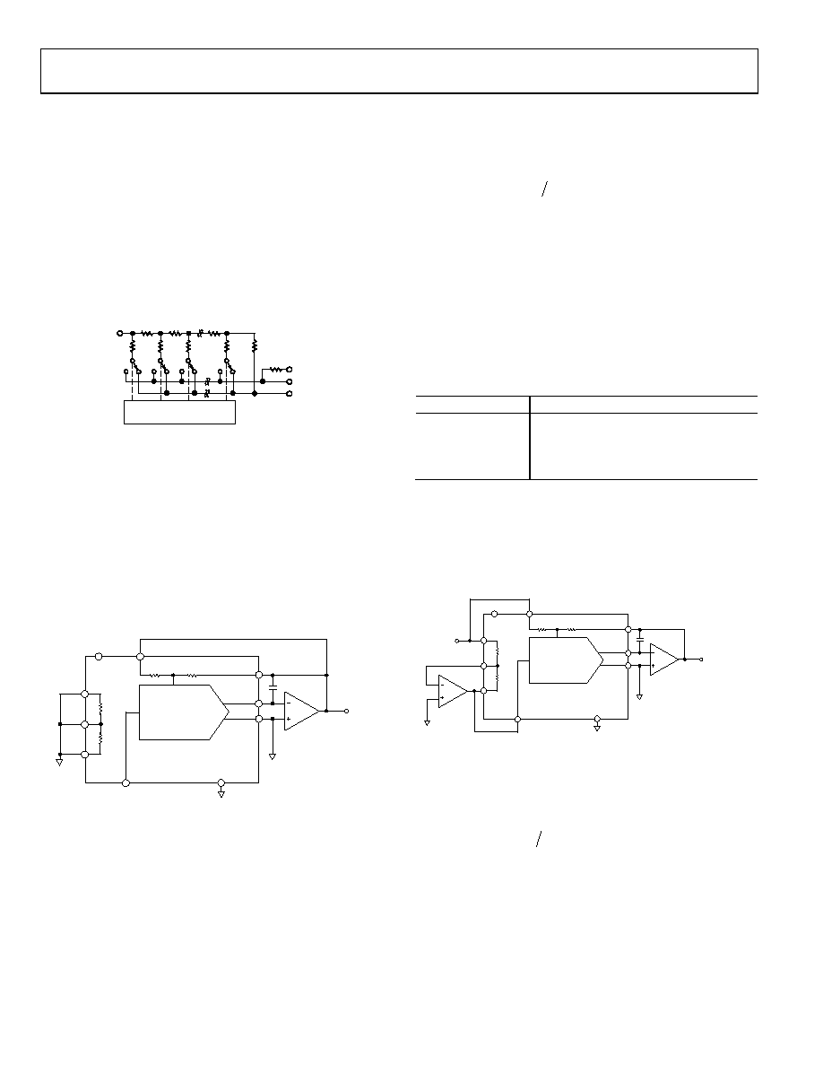
The AD5405 is a 12-bit, dual-channel, current-output DAC
consisting of a standard inverting R-2R ladder configuration.
Figure 31 shows a simplified diagram for a single channel of the
AD5405. The feedback resistor RFBA has a value of 2R. The
value of R is typically 10 kΩ (with a minimum of 8 kΩ and a
maximum of 13 kΩ). If IOUT1A and IOUT2A are kept at the same
potential, a constant current flows into each ladder leg,
regardless of digital input code. Therefore, the input resistance
presented at VREFA is always constant.
VREFA
IOUT 2A
DAC DATA LATCHES
AND DRIVERS
2R
S1
2R
S2
2R
S3
2R
S12
2R
R
IOUT1A
RFB A
R
04463-005
Figure 31. Simplified Ladder Configuration
Access is provided to the VREF, RFB, IOUT1, and IOUT2 terminals of
the DAC, making the device extremely versatile and allowing it
to be configured for several operating modes, such as unipolar
output, bipolar output, or single-supply mode.
CIRCUIT OPERATION
Unipolar Mode
Using a single op amp, this DAC can easily be configured to
provide 2-quadrant multiplying operation or a unipolar output
voltage swing, as shown in Figure 32.
RFB
2R
R1
2R
AD5405
12-Bit DAC A
R
R1A
RFBA
VDD
VREFA
VOUT = 0V TO –VIN
A1
IOUT2A
IOUT1A
AGND
C1
GND
AGND
R2A
R2_3A
R3A
R2
2R
R3
2R
AGND
04463-
006
NOTES
1. SIMILAR CONFIGURATION FOR DAC B.
2. C1 PHASE COMPENSATION (1pF TO 2pF) MAY BE REQUIRED
IF A1 IS A HIGH SPEED AMPLIFIER.
Figure 32. Unipolar Operation
When an output amplifier is connected in unipolar mode, the
output voltage is given by
n
REF
OUT
D
V
2
×
=
where:
D
is the fractional representation, in the range of 0 to 4,095, of
the digital word loaded to the DAC.
n
is the resolution of the DAC.
With a fixed 10 V reference, the circuit shown in Figure 32 gives
a unipolar 0 V to 10 V output voltage swing. When VIN is an ac
signal, the circuit performs 2-quadrant multiplication.
Table 5 shows the relationship between digital code and the
expected output voltage for unipolar operation.
Table 5. Unipolar Code
Digital Input
Analog Output (V)
1111 1111 1111
VREF (4,095/4,096)
1000 0000 0000
VREF (2,048/4,096) = VREF/2
0000 0000 0001
VREF (1/4,096)
0000 0000 0000
VREF (0/4,096) = 0
Bipolar Operation
In some applications, it may be necessary to generate full
4-quadrant multiplying operation or a bipolar output swing.
This can be easily accomplished by using another external
amplifier, as shown in Figure 33.
RFB
2R
R1
2R
AD5405
12-Bit DAC A
R
R1A
RFBA
VDD
VREFA
R2A
R2_3A
R3A
A1
IOUT2A
IOUT1A
AGND
C1
R2
2R
R3
2R
AGND
GND
AGND
A1
VIN
VOUT =–VIN TO +VIN
04463-
007
NOTES
1. SIMILAR CONFIGURATION FOR DAC B.
2. C1 PHASE COMPENSATION (1pF TO 2pF) MAY BE REQUIRED
IF A1 IS A HIGH SPEED AMPLIFIER.
Figure 33. Bipolar Operation (4-Quadrant Multiplication)
When in bipolar mode, the output voltage is given by
REF
n
REF
OUT
V
D
V
×
=
)
2
(
1
where:
D
is the fractional representation, in the range of 0 to 4,095, of
the digital word loaded to the DAC.
n
is the number of bits.
When VIN is an ac signal, the circuit performs 4-quadrant
multiplication.
相关PDF资料 |
PDF描述 |
|---|---|
| AD5415YRU | IC DAC DUAL 12BIT MULT 24-TSSOP |
| AD5421CREZ | IC DAC 16BIT SPI/SRL 28TSSOP |
| AD5422ACPZ-REEL7 | IC DAC 16BIT SRL 40LFCSP |
| AD5441BRMZ-REEL7 | IC DAC 12BIT SERIAL IN 8MSOP |
| AD5445YRU | IC DAC 12BIT PARALL IOUT 20TSSOP |
相关代理商/技术参数 |
参数描述 |
|---|---|
| AD540J | 制造商:未知厂家 制造商全称:未知厂家 功能描述:Analog IC |
| AD540JH | 制造商:AD84/07 功能描述:Operational Amplifier, Single AMP, Bipolar/JFET, 8 Pin, Metal Can |
| AD540K | 制造商:未知厂家 制造商全称:未知厂家 功能描述:Analog IC |
| AD540S | 制造商:未知厂家 制造商全称:未知厂家 功能描述:Analog IC |
| AD5410 | 制造商:AD 制造商全称:Analog Devices 功能描述:Low Power HART Modem |
发布紧急采购,3分钟左右您将得到回复。