参数资料
| 型号: | AD5410ACPZ-REEL |
| 厂商: | Analog Devices Inc |
| 文件页数: | 13/32页 |
| 文件大小: | 0K |
| 描述: | IC DAC 12BIT SRL 40LFCSP |
| 设计资源: | Simplified 12-Bit, 4 mA-to-20 mA Output Solution Using AD5410 (CN0081) |
| 标准包装: | 2,500 |
| 设置时间: | 40µs |
| 位数: | 12 |
| 数据接口: | DSP,MICROWIRE?,QSPI?,串行,SPI? |
| 转换器数目: | 1 |
| 电压电源: | 模拟和数字 |
| 功率耗散(最大): | 950mW |
| 工作温度: | -40°C ~ 85°C |
| 安装类型: | 表面贴装 |
| 封装/外壳: | 40-VFQFN 裸露焊盘,CSP |
| 供应商设备封装: | 40-LFCSP-VQ(6x6) |
| 包装: | 带卷 (TR) |
| 输出数目和类型: | 1 电流,单极 |
| 采样率(每秒): | * |
第1页第2页第3页第4页第5页第6页第7页第8页第9页第10页第11页第12页当前第13页第14页第15页第16页第17页第18页第19页第20页第21页第22页第23页第24页第25页第26页第27页第28页第29页第30页第31页第32页
AD5410/AD5420
Data Sheet
Rev. F | Page 20 of 32
POWER-ON STATE
circuit ensures that all registers are loaded with zero code. As
such, the output is disabled (tristate). Also upon power-on,
internal calibration registers are read, and the data is applied to
internal calibration circuitry. For a reliable read operation, there
must be sufficient voltage on the AVDD supply when the read event
is triggered by the DVCC power supply powering up. Powering
up the DVCC supply after the AVDD supply ensures this. If DVCC
and AVDD are powered up simultaneously or if the internal DVCC
is enabled, the supplies should be powered up at a rate greater
than, typically, 500 V/sec or 24 V per 50 ms. If this cannot be
after power-on. This performs a power-on reset event, reading
the calibration registers and ensuring specified operation of the
TRANSFER FUNCTION
For the 0 mA to 20 mA, 0 mA to 24 mA, and 4 mA to 20 mA
current output ranges, the output current is respectively
expressed as
D
I
N
OUT
2
mA
20
D
I
N
OUT
2
mA
24
mA
4
2
mA
16
D
I
N
OUT
where:
D
is the decimal equivalent of the code loaded to the DAC.
N
is the bit resolution of the DAC.
DATA REGISTER
The data register is addressed by setting the address byte of the
input shift register to 0x01. The data to be written to the data
register is entered in Position DB15 to Position DB4 for the
as shown in Table 12 and Table 13, respectively.
CONTROL REGISTER
The control register is addressed by setting the address byte of
the input shift register to 0x55. The data to be written to the
control register is entered in Position DB15 to Position DB0,
as shown in Table 14. The control register bit functions are
described in Table 10.
Table 10. Control Register Bit Functions
Bit
Description
REXT
Setting this bit selects the external current setting
for further details. When using an external current
setting resistor, it is recommended to only set REXT
when also setting the OUTEN bit. Alternately, REXT
can be set before the OUTEN bit is set, but the range
(see Table 11) must be changed on the write in which
the output is enabled. See Figure 40 for best practice.
OUTEN
Output enable. This bit must be set to enable the
output.
SR Clock
Features section.
SR Step
Features section.
SREN
Digital slew rate control enable.
DCEN
Daisy-chain enable.
R2, R1, R0
Output range select. See Table 11.
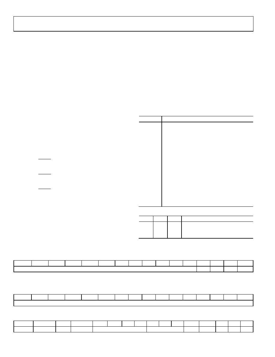
Table 11. Output Range Options
R2
R1
R0
Output Range Selected
1
0
1
4 mA to 20 mA current range
1
0
0 mA to 20 mA current range
1
0 mA to 24 mA current range
Table 12. Programming the AD5410 Data Register
MSB
LSB
DB15
DB14
DB13
DB12
DB11
DB10
DB9
DB8
DB7
DB6
DB5
DB4
DB3
DB2
DB1
DB0
12-bit data-word
1 X = don’t care.
Table 13. Programming the AD5420 Data Register
MSB
LSB
DB15
DB14
DB13
DB12
DB11
DB10
DB9
DB8
DB7
DB6
DB5
DB4
DB3
DB2
DB1
DB0
16-bit data-word
Table 14. Programming the Control Register
MSB
LSB
DB15
DB14
DB13
DB12
DB11
DB10
DB9
DB8
DB7
DB6
DB5
DB4
DB3
DB2
DB1
DB0
0
REXT
OUTEN
SR clock
SR step
SREN
DCEN
R2
R1
R0
相关PDF资料 |
PDF描述 |
|---|---|
| V300A2H160B | CONVERTER MOD DC/DC 2V 160W |
| V150A28H400BG | CONVERTER MOD DC/DC 28V 400W |
| VI-2N0-MW-F1 | CONVERTER MOD DC/DC 5V 100W |
| V150A28H400BF2 | CONVERTER MOD DC/DC 28V 400W |
| VI-23M-IV-S | CONVERTER MOD DC/DC 10V 150W |
相关代理商/技术参数 |
参数描述 |
|---|---|
| AD5410ACPZ-REEL7 | 功能描述:IC DAC 12BIT SRL 40LFCSP RoHS:是 类别:集成电路 (IC) >> 数据采集 - 数模转换器 系列:- 标准包装:1 系列:- 设置时间:4.5µs 位数:12 数据接口:串行,SPI? 转换器数目:1 电压电源:单电源 功率耗散(最大):- 工作温度:-40°C ~ 125°C 安装类型:表面贴装 封装/外壳:8-SOIC(0.154",3.90mm 宽) 供应商设备封装:8-SOICN 包装:剪切带 (CT) 输出数目和类型:1 电压,单极;1 电压,双极 采样率(每秒):* 其它名称:MCP4921T-E/SNCTMCP4921T-E/SNRCTMCP4921T-E/SNRCT-ND |
| AD5410AREZ | 功能描述:IC DAC 12BIT 1CH SER 24TSSOP RoHS:是 类别:集成电路 (IC) >> 数据采集 - 数模转换器 系列:- 产品培训模块:Lead (SnPb) Finish for COTS Obsolescence Mitigation Program 标准包装:50 系列:- 设置时间:4µs 位数:12 数据接口:串行 转换器数目:2 电压电源:单电源 功率耗散(最大):- 工作温度:-40°C ~ 85°C 安装类型:表面贴装 封装/外壳:8-TSSOP,8-MSOP(0.118",3.00mm 宽) 供应商设备封装:8-uMAX 包装:管件 输出数目和类型:2 电压,单极 采样率(每秒):* 产品目录页面:1398 (CN2011-ZH PDF) |
| AD5410AREZ-REEL7 | 功能描述:IC DAC 12BIT 1CH SER 24TSSOP RoHS:是 类别:集成电路 (IC) >> 数据采集 - 数模转换器 系列:- 产品培训模块:LTC263x 12-, 10-, and 8-Bit VOUT DAC Family 特色产品:LTC2636 - Octal 12-/10-/8-Bit SPI VOUT DACs with 10ppm/°C Reference 标准包装:91 系列:- 设置时间:4µs 位数:10 数据接口:MICROWIRE?,串行,SPI? 转换器数目:8 电压电源:单电源 功率耗散(最大):2.7mW 工作温度:-40°C ~ 85°C 安装类型:表面贴装 封装/外壳:14-WFDFN 裸露焊盘 供应商设备封装:14-DFN-EP(4x3) 包装:管件 输出数目和类型:8 电压,单极 采样率(每秒):* |
| AD5412 | 制造商:AD 制造商全称:Analog Devices 功能描述:Low Power HART Modem |
| AD5412_09 | 制造商:AD 制造商全称:Analog Devices 功能描述:Single Channel, 12-/16-Bit, Serial Input, Current Source and Voltage Output DACs |
发布紧急采购,3分钟左右您将得到回复。