参数资料
| 型号: | AD5415YRU |
| 厂商: | Analog Devices Inc |
| 文件页数: | 9/29页 |
| 文件大小: | 0K |
| 描述: | IC DAC DUAL 12BIT MULT 24-TSSOP |
| 产品培训模块: | Data Converter Fundamentals DAC Architectures |
| 标准包装: | 62 |
| 设置时间: | 120ns |
| 位数: | 12 |
| 数据接口: | 串行 |
| 转换器数目: | 2 |
| 电压电源: | 单电源 |
| 功率耗散(最大): | 3.5µW |
| 工作温度: | -40°C ~ 125°C |
| 安装类型: | 表面贴装 |
| 封装/外壳: | 24-TSSOP(0.173",4.40mm 宽) |
| 供应商设备封装: | 24-TSSOP |
| 包装: | 管件 |
| 输出数目和类型: | 4 电流,单极;4 电流,双极 |
| 采样率(每秒): | 2.47M |
第1页第2页第3页第4页第5页第6页第7页第8页当前第9页第10页第11页第12页第13页第14页第15页第16页第17页第18页第19页第20页第21页第22页第23页第24页第25页第26页第27页第28页第29页
AD5415
Data Sheet
Rev. E | Page 16 of 28
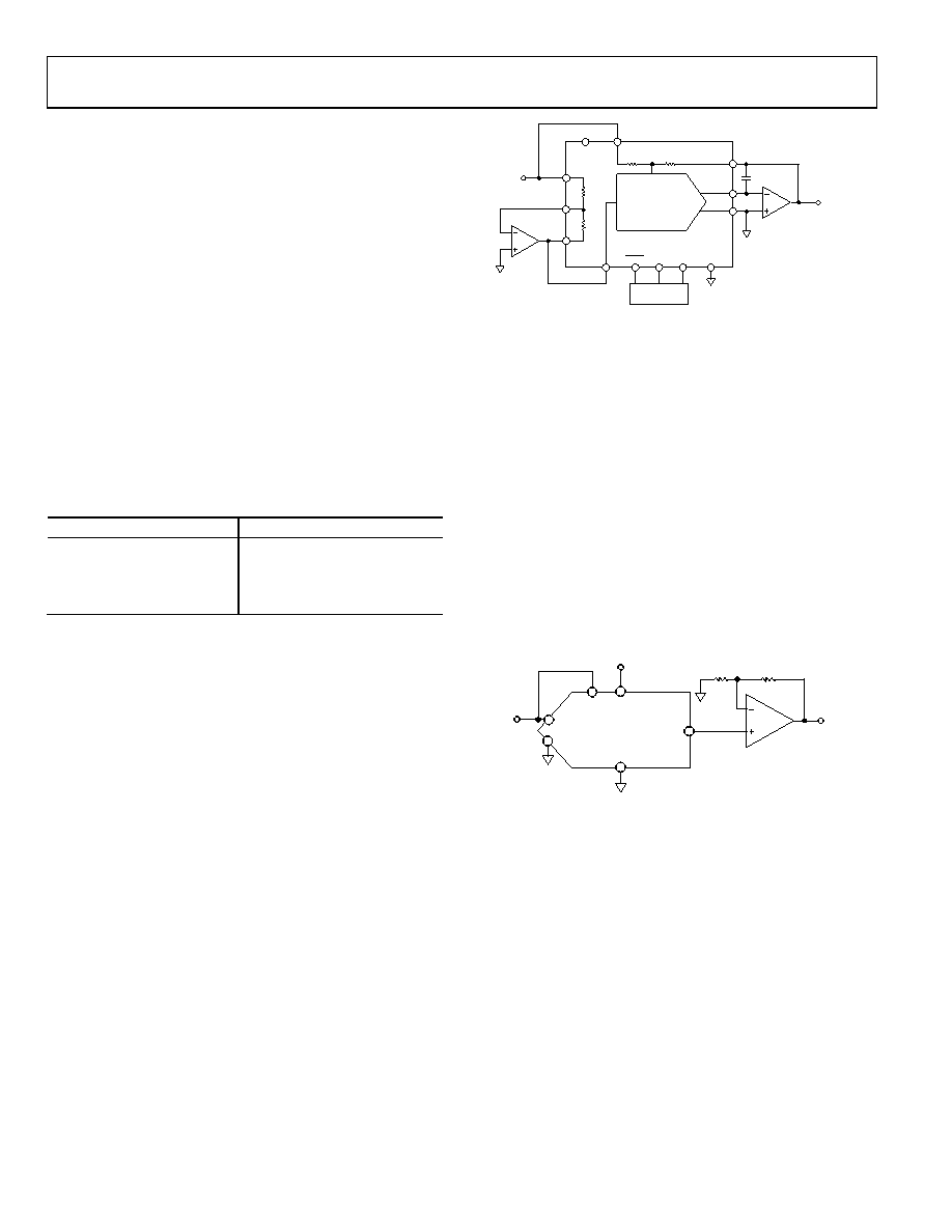
Bipolar Operation
In some applications, it may be necessary to generate full
4-quadrant multiplying operation or a bipolar output swing.
This can easily be accomplished by using another external
amplifier and the on-chip 4-quadrant resistors, as shown in
When in bipolar mode, the output voltage is given by
VOUT = (VREF × D/2n 1) VREF
where:
D is the fractional representation, in the range of 0 to 4,095, of
the digital word loaded to the DAC.
n is the number of bits.
When VIN is an ac signal, the circuit performs 4-quadrant
multiplication.
Table 6 shows the relationship between digital code and the
expected output voltage for bipolar operation.
Table 6. Bipolar Code
Digital Input
Analog Output (V)
1111 1111 1111
+VREF (4,095/4,096)
1000 0000 0000
0
0000 0000 0001
VREF (4,095/4,096)
0000 0000 0000
VREF (4,096/4,096)
Stability
In the I-to-V configuration, the IOUT of the DAC and the
inverting node of the op amp must be connected as close as
possible, and proper PCB layout techniques must be used.
Because every code change corresponds to a step function, gain
peaking may occur if the op amp has limited gain bandwidth
product (GBP) and there is excessive parasitic capacitance at the
inverting node. This parasitic capacitance introduces a pole into
the open-loop response, which can cause ringing or instability
in the closed-loop applications circuit.
An optional compensation capacitor, C1, can be added in
Figure 35. Too small a value of C1 can produce ringing at
the output, whereas too large a value can adversely affect the
settling time. C1 should be found empirically, but 1 pF to 2 pF
is generally adequate for the compensation.
IOUT1A
IOUT2A
RFBA
RFB
2R
R1
2R
AD5415
12-BIT DAC A
R
GND
SDIN
VREFA
SCLK
SYNC
R2
2R
R3
2R
R2A
R2_3A
R3A
VDD
C1
A1
VOUT = –VIN TO +VIN
A1
AGND
CONTROLLER
R1A
AGND
VIN
04461-034
NOTES
1. DAC B OMITTED FOR CLARITY.
2. C1 PHASE COMPENSATION (1pF TO 2pF) MAY BE REQUIRED
IF A1 IS A HIGH SPEED AMPLIFIER.
Figure 35. Bipolar Operation
SINGLE-SUPPLY APPLICATIONS
Voltage-Switching Mode of Operation
Figure 36 shows the DAC operating in the voltage-switching
mode. The reference voltage, VIN, is applied to the IOUT1A pin,
IOUT2A is connected to AGND, and the output voltage is
available at the VREFA terminal. In this configuration, a positive
reference voltage results in a positive output voltage, making
single-supply operation possible. The output from the DAC is
voltage at a constant impedance (the DAC ladder resistance).
Therefore, an op amp is necessary to buffer the output voltage.
The reference input no longer sees a constant input impedance,
but one that varies with code. Therefore, the voltage input
should be driven from a low impedance source.
04461-035
VOUT
VDD
GND
VIN
IOUT2A
IOUT1A
RFBA VDD
VREFA
R2
R1
NOTES
1. SIMILAR CONFIGURATION FOR DACB
2. C1 PHASE COMPENSATION (1pF TO 2pF) MAY BE REQUIRED
IF A1 IS A HIGH SPEED AMPLIFIER.
Figure 36. Single-Supply Voltage-Switching Mode
Note that VIN is limited to low voltages because the switches in
the DAC ladder no longer have the same source-drain drive
voltage. As a result, their on resistance differs and degrades the
integral linearity of the DAC. Also, VIN must not go negative by
more than 0.3 V, or an internal diode turns on, causing the device
to exceed the maximum ratings. In this type of application, the
full range of multiplying capability of the DAC is lost.
相关PDF资料 |
PDF描述 |
|---|---|
| AD5421CREZ | IC DAC 16BIT SPI/SRL 28TSSOP |
| AD5422ACPZ-REEL7 | IC DAC 16BIT SRL 40LFCSP |
| AD5441BRMZ-REEL7 | IC DAC 12BIT SERIAL IN 8MSOP |
| AD5445YRU | IC DAC 12BIT PARALL IOUT 20TSSOP |
| AD5446YRM | IC DAC 14BIT MULTIPLYING 10-MSOP |
相关代理商/技术参数 |
参数描述 |
|---|---|
| AD5415YRU-REEL | 制造商:Analog Devices 功能描述:DAC 2-CH R-2R 12-bit 24-Pin TSSOP T/R 制造商:Analog Devices 功能描述:DAC 2CH R-2R 12-BIT 24TSSOP - Tape and Reel |
| AD5415YRU-REEL7 | 功能描述:IC DAC DUAL 12BIT MULT 24-TSSOP RoHS:否 类别:集成电路 (IC) >> 数据采集 - 数模转换器 系列:- 产品培训模块:LTC263x 12-, 10-, and 8-Bit VOUT DAC Family 特色产品:LTC2636 - Octal 12-/10-/8-Bit SPI VOUT DACs with 10ppm/°C Reference 标准包装:91 系列:- 设置时间:4µs 位数:10 数据接口:MICROWIRE?,串行,SPI? 转换器数目:8 电压电源:单电源 功率耗散(最大):2.7mW 工作温度:-40°C ~ 85°C 安装类型:表面贴装 封装/外壳:14-WFDFN 裸露焊盘 供应商设备封装:14-DFN-EP(4x3) 包装:管件 输出数目和类型:8 电压,单极 采样率(每秒):* |
| AD5415YRUZ | 功能描述:IC DAC DUAL 12BIT MULT 24-TSSOP RoHS:是 类别:集成电路 (IC) >> 数据采集 - 数模转换器 系列:- 产品培训模块:Lead (SnPb) Finish for COTS Obsolescence Mitigation Program 标准包装:50 系列:- 设置时间:4µs 位数:12 数据接口:串行 转换器数目:2 电压电源:单电源 功率耗散(最大):- 工作温度:-40°C ~ 85°C 安装类型:表面贴装 封装/外壳:8-TSSOP,8-MSOP(0.118",3.00mm 宽) 供应商设备封装:8-uMAX 包装:管件 输出数目和类型:2 电压,单极 采样率(每秒):* 产品目录页面:1398 (CN2011-ZH PDF) |
| AD5415YRUZ-REEL | 功能描述:IC DAC 12BIT DUAL MULT 24-TSSOP RoHS:是 类别:集成电路 (IC) >> 数据采集 - 数模转换器 系列:- 产品培训模块:LTC263x 12-, 10-, and 8-Bit VOUT DAC Family 特色产品:LTC2636 - Octal 12-/10-/8-Bit SPI VOUT DACs with 10ppm/°C Reference 标准包装:91 系列:- 设置时间:4µs 位数:10 数据接口:MICROWIRE?,串行,SPI? 转换器数目:8 电压电源:单电源 功率耗散(最大):2.7mW 工作温度:-40°C ~ 85°C 安装类型:表面贴装 封装/外壳:14-WFDFN 裸露焊盘 供应商设备封装:14-DFN-EP(4x3) 包装:管件 输出数目和类型:8 电压,单极 采样率(每秒):* |
| AD5415YRUZ-REEL7 | 功能描述:IC DAC 12BIT DUAL MULT 24-TSSOP RoHS:是 类别:集成电路 (IC) >> 数据采集 - 数模转换器 系列:- 产品培训模块:LTC263x 12-, 10-, and 8-Bit VOUT DAC Family 特色产品:LTC2636 - Octal 12-/10-/8-Bit SPI VOUT DACs with 10ppm/°C Reference 标准包装:91 系列:- 设置时间:4µs 位数:10 数据接口:MICROWIRE?,串行,SPI? 转换器数目:8 电压电源:单电源 功率耗散(最大):2.7mW 工作温度:-40°C ~ 85°C 安装类型:表面贴装 封装/外壳:14-WFDFN 裸露焊盘 供应商设备封装:14-DFN-EP(4x3) 包装:管件 输出数目和类型:8 电压,单极 采样率(每秒):* |
发布紧急采购,3分钟左右您将得到回复。