参数资料
| 型号: | AD5420ACPZ-REEL7 |
| 厂商: | Analog Devices Inc |
| 文件页数: | 10/32页 |
| 文件大小: | 0K |
| 描述: | IC DAC 16BIT SRL 40LFCSP |
| 设计资源: | Simplified 16-Bit, 4 mA-to-20 mA Output Solution Using AD5420 (CN0098) |
| 标准包装: | 1 |
| 设置时间: | 10µs |
| 位数: | 16 |
| 数据接口: | DSP,MICROWIRE?,QSPI?,串行,SPI? |
| 转换器数目: | 1 |
| 电压电源: | 模拟和数字 |
| 功率耗散(最大): | 950mW |
| 工作温度: | -40°C ~ 85°C |
| 安装类型: | 表面贴装 |
| 封装/外壳: | 40-VFQFN 裸露焊盘,CSP |
| 供应商设备封装: | 40-LFCSP-VQ(6x6) |
| 包装: | 标准包装 |
| 输出数目和类型: | 1 电流,单极 |
| 采样率(每秒): | * |
| 其它名称: | AD5420ACPZ-REEL7DKR |
第1页第2页第3页第4页第5页第6页第7页第8页第9页当前第10页第11页第12页第13页第14页第15页第16页第17页第18页第19页第20页第21页第22页第23页第24页第25页第26页第27页第28页第29页第30页第31页第32页
AD5410/AD5420
Data Sheet
Rev. F | Page 18 of 32
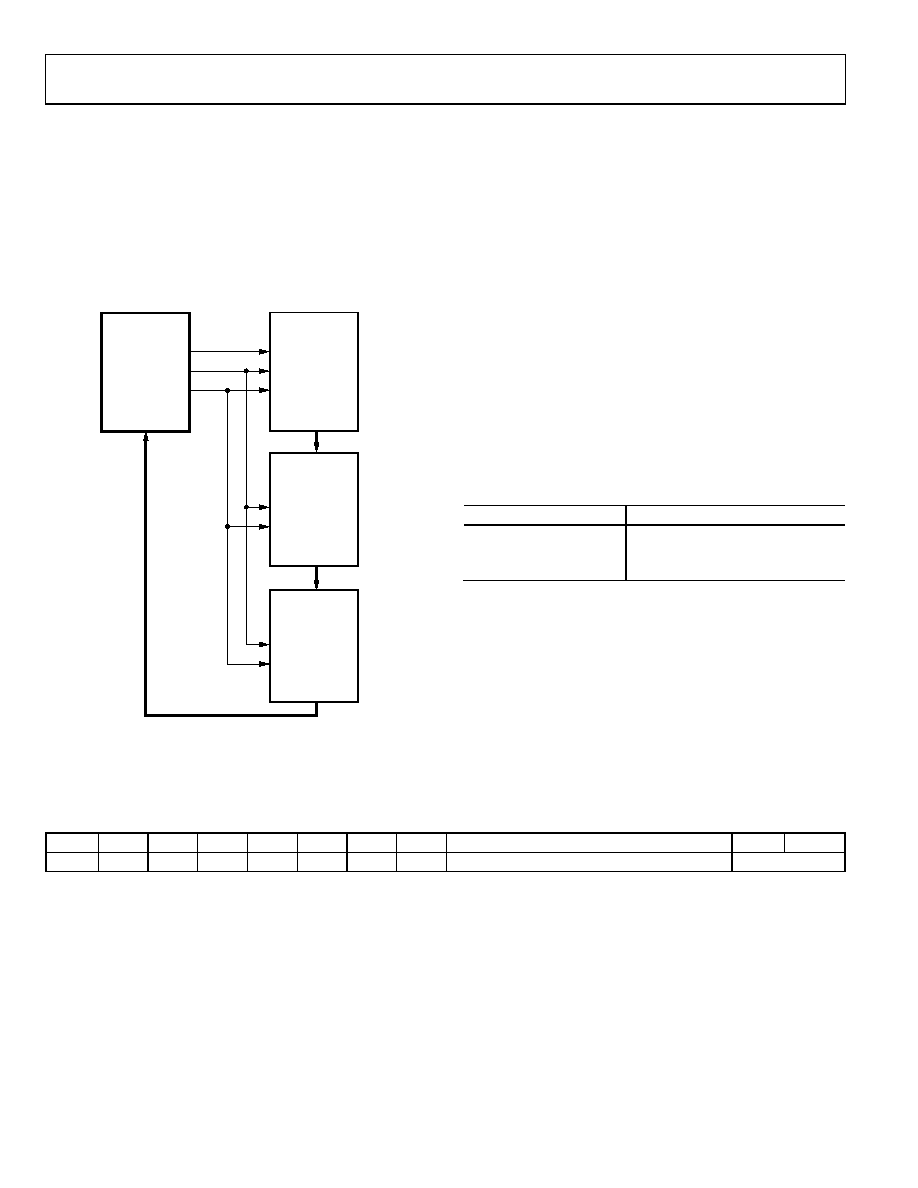
chain. When the serial transfer to all devices is complete,
LATCH is taken high. This latches the input data in each device
in the daisy chain. The serial clock can be a continuous or a
gated clock.
A continuous SCLK source can be used only if LATCH is taken
high after the correct number of clock cycles. In gated clock
mode, a burst clock containing the exact number of clock cycles
must be used, and LATCH must be taken high after the final
clock to latch the data. See Figure 4 for a timing diagram.
CONTROLLER
DATA IN
LATCH
SDIN
SCLK
DATA OUT
SERIAL CLOCK
CONTROL OUT
SDO
LATCH
SCLK
SDO
LATCH
SCLK
SDO
SDIN
*ADDITIONAL PINS OMITTED FOR CLARITY.
AD5410/
AD5420*
AD5410/
AD5420*
AD5410/
AD5420*
07027-
035
Readback Operation
Readback mode is invoked by setting the address byte and read
should be a NOP command, which clocks out the data from the
previously addressed register, as shown in Figure 3. By default,
the SDO pin is disabled. After having addressed the AD5410/
AD5420 for a read operation, a rising edge on LATCH enables
the SDO pin in anticipation of data being clocked out. After the
data has been clocked out on SDO, a rising edge on LATCH
disables (tristate) the SDO pin once again. To read back the
data register, for example, the following sequence should be
implemented:
register. This configures the part for read mode with the
data register selected.
2. Follow this with a second write, a NOP condition, 0x000000.
During this write, the data from the data register is clocked
out on the SDO line.
Table 8. Read Address Decoding
Read Address
Function
00
Read status register
01
Read data register
10
Read control register
Table 9. Input Shift Register Contents for a Read Operation
MSB
LSB
DB23
DB22
DB21
DB20
DB19
DB18
DB17
DB16
DB15 to DB2
DB1
DB0
0
1
0
Read address
1
X = don’t care.
相关PDF资料 |
PDF描述 |
|---|---|
| SY89876LMI | IC CLK BUFF DVDR 1:2 2GHZ 16-MLF |
| LTC2642CMS-14#TRPBF | IC DAC 14BIT VOUT 10-MSOP |
| LTC2642CDD-14#TRPBF | IC DAC 14BIT VOUT 10-DFN |
| SY89875UMI | IC CLK BUFF DVDR 1:2 2GHZ 16-MLF |
| LTC2641CMS8-14#TRPBF | IC DAC 14BIT VOUT 8-MSOP |
相关代理商/技术参数 |
参数描述 |
|---|---|
| AD5420AREZ | 功能描述:IC DAC 16BIT 1CH SER 24TSSOP RoHS:是 类别:集成电路 (IC) >> 数据采集 - 数模转换器 系列:- 产品培训模块:Lead (SnPb) Finish for COTS Obsolescence Mitigation Program 标准包装:50 系列:- 设置时间:4µs 位数:12 数据接口:串行 转换器数目:2 电压电源:单电源 功率耗散(最大):- 工作温度:-40°C ~ 85°C 安装类型:表面贴装 封装/外壳:8-TSSOP,8-MSOP(0.118",3.00mm 宽) 供应商设备封装:8-uMAX 包装:管件 输出数目和类型:2 电压,单极 采样率(每秒):* 产品目录页面:1398 (CN2011-ZH PDF) |
| AD5420AREZ-REEL7 | 功能描述:IC DAC 16BIT 1CH SER 24TSSOP RoHS:是 类别:集成电路 (IC) >> 数据采集 - 数模转换器 系列:- 标准包装:47 系列:- 设置时间:2µs 位数:14 数据接口:并联 转换器数目:1 电压电源:单电源 功率耗散(最大):55µW 工作温度:-40°C ~ 85°C 安装类型:表面贴装 封装/外壳:28-SSOP(0.209",5.30mm 宽) 供应商设备封装:28-SSOP 包装:管件 输出数目和类型:1 电流,单极;1 电流,双极 采样率(每秒):* |
| AD5420BCPZ | 制造商:AD 制造商全称:Analog Devices 功能描述:Single Channel, 16-Bit, Serial Input, Current Source DAC |
| AD5420BREZ | 制造商:Analog Devices 功能描述: |
| AD5421 | 制造商:AD 制造商全称:Analog Devices 功能描述:Low Power HART Modem |
发布紧急采购,3分钟左右您将得到回复。