参数资料
| 型号: | AD5420ACPZ-REEL |
| 厂商: | Analog Devices Inc |
| 文件页数: | 9/32页 |
| 文件大小: | 0K |
| 描述: | IC DAC 16BIT SRL 40LFCSP |
| 设计资源: | Simplified 16-Bit, 4 mA-to-20 mA Output Solution Using AD5420 (CN0098) |
| 标准包装: | 2,500 |
| 设置时间: | 10µs |
| 位数: | 16 |
| 数据接口: | DSP,MICROWIRE?,QSPI?,串行,SPI? |
| 转换器数目: | 1 |
| 电压电源: | 模拟和数字 |
| 功率耗散(最大): | 950mW |
| 工作温度: | -40°C ~ 85°C |
| 安装类型: | 表面贴装 |
| 封装/外壳: | 40-VFQFN 裸露焊盘,CSP |
| 供应商设备封装: | 40-LFCSP-VQ(6x6) |
| 包装: | 带卷 (TR) |
| 输出数目和类型: | 1 电流,单极 |
| 采样率(每秒): | * |
第1页第2页第3页第4页第5页第6页第7页第8页当前第9页第10页第11页第12页第13页第14页第15页第16页第17页第18页第19页第20页第21页第22页第23页第24页第25页第26页第27页第28页第29页第30页第31页第32页
Data Sheet
AD5410/AD5420
Rev. F | Page 17 of 32
THEORY OF OPERATION
The AD5410/AD5420 are precision digital-to-current loop output
converters designed to meet the requirements of industrial
process control applications. They provide a high precision,
fully integrated, low cost single-chip solution for generating
current loop outputs. The current ranges available are 0 mA
to 20 mA, 0 mA to 24 mA, and 4 mA to 20 mA. The desired
output configuration is user selectable via the control register.
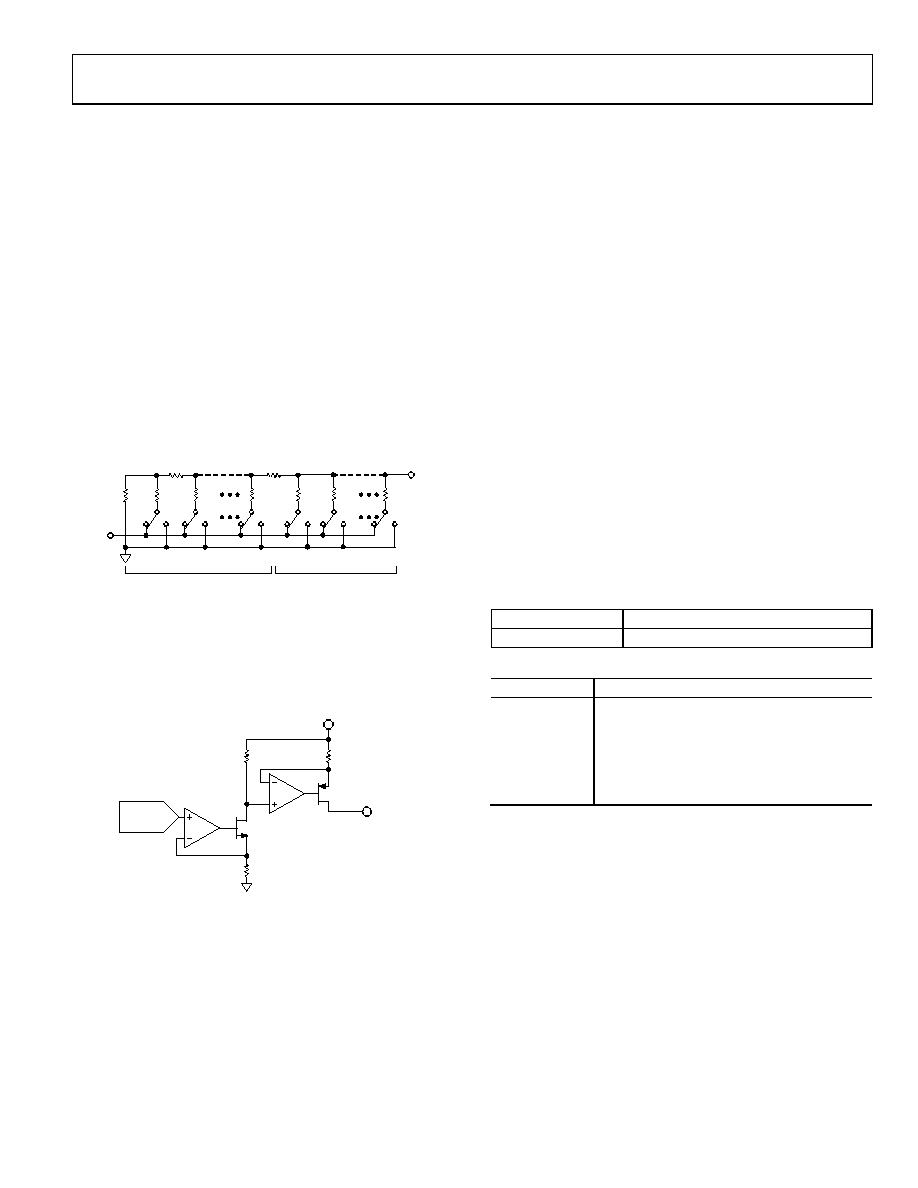
ARCHITECTURE
two matched DAC sections. A simplified circuit diagram is shown
in Figure 37. The four MSBs of the 12-bit or 16-bit data-word
are decoded to drive 15 switches, E1 to E15. Each of these switches
connects one of 15 matched resistors to either ground or the
reference buffer output. The remaining 8/12 bits of the data-
word drive Switch S0 to Switch S7 or Switch S0 to Switch S11 of an
8-/12-bit voltage mode R-2R ladder network.
2R
S0
VREFIN
2R
S1
2R
S7/S11
2R
E1
2R
E2
2R
E15
2R
VOUT
8-/12-BIT R-2R LADDER
FOUR MSBs DECODED INTO
15 EQUAL SEGMENTS
07027-
033
Figure 37. DAC Ladder Structure
The voltage output from the DAC core is converted to a current
(see Figure 38) that is then mirrored to the supply rail so that
the application simply sees a current source output with respect
to ground.
R2
RSET
T1
T2
A1
R3
IOUT
AVDD
12-/16-BIT
DAC
07027-
034
A2
Figure 38. Voltage-to-Current Conversion Circuitry
SERIAL INTERFACE
serial interface that operates at clock rates of up to 30 MHz. They
are compatible with SPI, QSPI, MICROWIRE, and DSP
standards.
Input Shift Register
The input shift register is 24 bits wide. Data is loaded into the
device MSB first as a 24-bit word under the control of a serial
clock input, SCLK. Data is clocked in on the rising edge of
SCLK. The input shift register consists of eight address bits and
16 data bits, as shown in Table 6. The 24-bit word is uncondition-
ally latched on the rising edge of LATCH. Data continues to be
clocked in irrespective of the state of LATCH. On the rising edge
of LATCH, the data that is present in the input shift register is
latched; that is, the last 24 bits to be clocked in before the rising
edge of LATCH is the data that is latched. The timing diagram
for this operation is shown in Figure 2.
Standalone Operation
The serial interface works with both a continuous and noncon-
tinuous SCLK. A continuous SCLK source can be used only if
LATCH is taken high after the correct number of data bits has
been clocked in. In gated clock mode, a burst clock containing
the exact number of clock cycles must be used, and LATCH
must be taken high after the final clock to latch the data. The
first rising edge of SCLK that clocks in the MSB of the data-
word marks the beginning of the write cycle. Exactly 24 rising
clock edges must be applied to SCLK before LATCH is brought
high. If LATCH is brought high before the 24th rising SCLK
edge, the data written is invalid. If more than 24 rising SCLK
edges are applied before LATCH is brought high, the input data
is also invalid.
Table 6. Input Shift Register Format
MSB
LSB
DB23 to DB16
DB15 to DB0
Address byte
Data-word
Table 7. Address Byte Functions
Address Byte
Function
00000000
No operation (NOP)
00000001
Data register
00000010
Readback register value as per read address
01010101
Control register
01010110
Reset register
Daisy-Chain Operation
For systems that contain several devices, the SDO pin can be used
to daisy-chain several devices together, as shown in Figure 39.
This daisy-chain mode can be useful in system diagnostics and
in reducing the number of serial interface lines. Daisy-chain
mode is enabled by setting the DCEN bit of the control register.
The first rising edge of SCLK that clocks in the MSB of the data-
word marks the beginning of the write cycle. SCLK is continuously
applied to the input shift register. If more than 24 clock pulses
are applied, the data ripples out of the input shift register and
appears on the SDO line. This data, having been clocked out on
the previous falling SCLK edge, is valid on the rising edge of
SCLK. By connecting the SDO of the first device to the SDIN
input of the next device in the chain, a multidevice interface is
constructed. Each device in the system requires 24 clock pulses.
Therefore, the total number of clock cycles must equal 24 × N,
相关PDF资料 |
PDF描述 |
|---|---|
| V300A28H500BG2 | CONVERTER MOD DC/DC 28V 500W |
| V300A24H500BG3 | CONVERTER MOD DC/DC 24V 500W |
| V300A24H500BG2 | CONVERTER MOD DC/DC 24V 500W |
| V300A24H500BF3 | CONVERTER MOD DC/DC 24V 500W |
| NBSG14MNHTBG | IC CLK/DATA BUFF 1:4 12GHZ 16QFN |
相关代理商/技术参数 |
参数描述 |
|---|---|
| AD5420ACPZ-REEL7 | 功能描述:IC DAC 16BIT SRL 40LFCSP RoHS:是 类别:集成电路 (IC) >> 数据采集 - 数模转换器 系列:- 标准包装:47 系列:- 设置时间:2µs 位数:14 数据接口:并联 转换器数目:1 电压电源:单电源 功率耗散(最大):55µW 工作温度:-40°C ~ 85°C 安装类型:表面贴装 封装/外壳:28-SSOP(0.209",5.30mm 宽) 供应商设备封装:28-SSOP 包装:管件 输出数目和类型:1 电流,单极;1 电流,双极 采样率(每秒):* |
| AD5420AREZ | 功能描述:IC DAC 16BIT 1CH SER 24TSSOP RoHS:是 类别:集成电路 (IC) >> 数据采集 - 数模转换器 系列:- 产品培训模块:Lead (SnPb) Finish for COTS Obsolescence Mitigation Program 标准包装:50 系列:- 设置时间:4µs 位数:12 数据接口:串行 转换器数目:2 电压电源:单电源 功率耗散(最大):- 工作温度:-40°C ~ 85°C 安装类型:表面贴装 封装/外壳:8-TSSOP,8-MSOP(0.118",3.00mm 宽) 供应商设备封装:8-uMAX 包装:管件 输出数目和类型:2 电压,单极 采样率(每秒):* 产品目录页面:1398 (CN2011-ZH PDF) |
| AD5420AREZ-REEL7 | 功能描述:IC DAC 16BIT 1CH SER 24TSSOP RoHS:是 类别:集成电路 (IC) >> 数据采集 - 数模转换器 系列:- 标准包装:47 系列:- 设置时间:2µs 位数:14 数据接口:并联 转换器数目:1 电压电源:单电源 功率耗散(最大):55µW 工作温度:-40°C ~ 85°C 安装类型:表面贴装 封装/外壳:28-SSOP(0.209",5.30mm 宽) 供应商设备封装:28-SSOP 包装:管件 输出数目和类型:1 电流,单极;1 电流,双极 采样率(每秒):* |
| AD5420BCPZ | 制造商:AD 制造商全称:Analog Devices 功能描述:Single Channel, 16-Bit, Serial Input, Current Source DAC |
| AD5420BREZ | 制造商:Analog Devices 功能描述: |
发布紧急采购,3分钟左右您将得到回复。