参数资料
| 型号: | AD5422ACPZ-REEL7 |
| 厂商: | Analog Devices Inc |
| 文件页数: | 28/44页 |
| 文件大小: | 0K |
| 描述: | IC DAC 16BIT SRL 40LFCSP |
| 设计资源: | 16-Bit Fully Isolated Output Module Using AD5422 and ADuM1401 (CN0065) Simplified 16-Bit Voltage Output and 4 mA-to-20 mA Output Solution Using AD5422 (CN0077) |
| 标准包装: | 1 |
| 设置时间: | 25µs |
| 位数: | 16 |
| 数据接口: | MICROWIRE?,串行,SPI? |
| 转换器数目: | 1 |
| 电压电源: | 模拟和数字,双 ± |
| 功率耗散(最大): | 950mW |
| 工作温度: | -40°C ~ 85°C |
| 安装类型: | 表面贴装 |
| 封装/外壳: | 40-VFQFN 裸露焊盘,CSP |
| 供应商设备封装: | 40-LFCSP-VQ(6x6) |
| 包装: | 标准包装 |
| 输出数目和类型: | 1 电流,单极;1 电流,双极;1 电压,单极;1 电压,双极 |
| 采样率(每秒): | 40k |
| 其它名称: | AD5422ACPZ-REEL7DKR |
第1页第2页第3页第4页第5页第6页第7页第8页第9页第10页第11页第12页第13页第14页第15页第16页第17页第18页第19页第20页第21页第22页第23页第24页第25页第26页第27页当前第28页第29页第30页第31页第32页第33页第34页第35页第36页第37页第38页第39页第40页第41页第42页第43页第44页
AD5412/AD5422
Data Sheet
Rev. I | Page 34 of 44
DIGITAL POWER SUPPLY
By default, the DVCC pin accepts a power supply of 2.7 V to
5.5 V. Alternatively, via the DVCC SELECT pin, an internal 4.5 V
power supply can be output on the DVCC pin for use as a digital
power supply for other devices in the system or as a termination
for pull-up resistors. This facility offers the advantage of not
having to bring a digital supply across an isolation barrier. The
internal power supply is enabled by leaving the DVCC SELECT
pin unconnected. To disable the internal supply, tie DVCC
SELECT to 0 V. DVCC is capable of supplying up to 5 mA of
current (for a load regulation graph, see Figure 10).
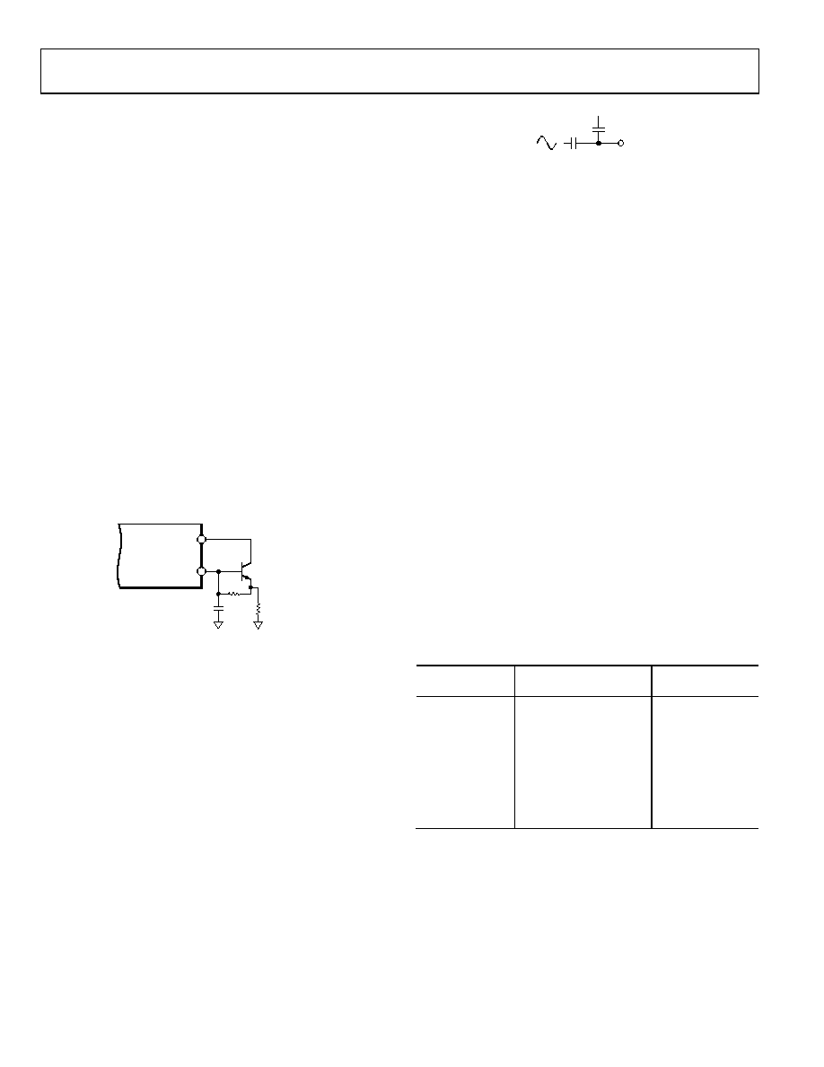
EXTERNAL BOOST FUNCTION
The addition of an external boost transistor, as shown in
by reducing the current flowing in the on-chip output transistor
(dividing it by the current gain of the external circuit). A
discrete NPN transistor with a breakdown voltage, BVCEO,
greater than 40 V can be used. The external boost capability
has been developed for users who may wish to use the AD5412/
AD5422 at the extremes of the supply voltage, load current, and
temperature range. The boost transistor can also be used to
reduce the amount of temperature-induced drift in the part.
This minimizes the temperature-induced drift of the on-chip
voltage reference, which improves on drift and linearity.
BOOST
MJD31C
OR
PBSS8110Z
RLOAD
0.022F
1k
AD5412/
AD5422
IOUT
06996-
061
Figure 70. External Boost Configuration
EXTERNAL COMPENSATION CAPACITOR
The voltage output can ordinarily drive capacitive loads of up to
20 nF; if there is a requirement to drive greater capacitive loads,
of up to 1 F, an external compensation capacitor can be con-
nected between the CCOMP and VOUT pins. The addition of the
capacitor keeps the output voltage stable but also reduces the
bandwidth and increases the settling time of the voltage output.
HART COMMUNICATION
pin, into which a HART signal can be coupled. The HART
signal appears on the current output if the output is enabled. To
achieve a 1 mA peak-to-peak current, the signal amplitude at
the CAP2 pin must be 48 mV peak-to-peak. Assuming that the
modem output amplitude is 500 mV peak-to-peak, its output
must be attenuated by 500/48 = 10.42. If this voltage is used, the
current output should meet the HART amplitude specifications.
Figure 71 shows the recommended circuit for attenuating and
coupling in the HART signal.
HART MODEM
OUTPUT
C1
C2
CAP2
AVDD
06996-
051
Figure 71. Coupling HART Signal
In determining the absolute values of the capacitors, ensure that
the FSK output from the modem is passed undistorted. Thus,
the bandwidth presented to the modem output signal must pass
1200 Hz and 2200 Hz frequencies. The recommended values
are C1 = 2.2 nF and C2 = 22 nF. Digitally controlling the slew
rate of the output is necessary to meet the analog rate of change
requirements for HART.
DIGITAL SLEW RATE CONTROL
user to control the rate at which the output voltage or current
changes. With the slew rate control feature disabled, the output
changes at a rate limited by the output drive circuitry and the
attached load. See Figure 64 for current output step and
Figure 38 for voltage output step. To reduce the slew rate, enable
the slew rate control feature. With the feature enabled via the
SREN bit of the control register (see Table 14), the output, instead
of slewing directly between two values, steps digitally at a rate
defined by two parameters accessible via the control register, as
shown in Table 14. The parameters are set by the SR clock and
SR step bits. SR clock defines the rate at which the digital slew is
updated; SR step defines by how much the output value changes
at each update. Both parameters together define the rate of
change of the output voltage or current. Table 22 and Table 23
outline the range of values for both the SR clock and SR step
parameters. Figure 72 shows the output current changing for
ramp times of 10 ms, 50 ms, and 100 ms.
Table 22. Slew Rate Step Size Options
SR Step
AD5412 Step Size
(LSB)
AD5422 Step
Size (LSB)
000
1/16
1
001
1/8
2
010
1/4
4
011
1/2
8
100
1
16
101
2
32
110
4
64
111
8
128
相关PDF资料 |
PDF描述 |
|---|---|
| AD5441BRMZ-REEL7 | IC DAC 12BIT SERIAL IN 8MSOP |
| AD5445YRU | IC DAC 12BIT PARALL IOUT 20TSSOP |
| AD5446YRM | IC DAC 14BIT MULTIPLYING 10-MSOP |
| AD5447YRU | IC DAC 12BIT DUAL MULT 24-TSSOP |
| AD5453YRM | IC DAC 14BIT MULTIPLYING 8-MSOP |
相关代理商/技术参数 |
参数描述 |
|---|---|
| AD5422AREZ | 功能描述:IC DAC 16BIT SER 24TSSOP RoHS:是 类别:集成电路 (IC) >> 数据采集 - 数模转换器 系列:- 产品培训模块:Lead (SnPb) Finish for COTS Obsolescence Mitigation Program 标准包装:50 系列:- 设置时间:4µs 位数:12 数据接口:串行 转换器数目:2 电压电源:单电源 功率耗散(最大):- 工作温度:-40°C ~ 85°C 安装类型:表面贴装 封装/外壳:8-TSSOP,8-MSOP(0.118",3.00mm 宽) 供应商设备封装:8-uMAX 包装:管件 输出数目和类型:2 电压,单极 采样率(每秒):* 产品目录页面:1398 (CN2011-ZH PDF) |
| AD5422AREZ-REEL | 功能描述:IC DAC 16BIT SRL 24TSSOP RoHS:是 类别:集成电路 (IC) >> 数据采集 - 数模转换器 系列:- 标准包装:47 系列:- 设置时间:2µs 位数:14 数据接口:并联 转换器数目:1 电压电源:单电源 功率耗散(最大):55µW 工作温度:-40°C ~ 85°C 安装类型:表面贴装 封装/外壳:28-SSOP(0.209",5.30mm 宽) 供应商设备封装:28-SSOP 包装:管件 输出数目和类型:1 电流,单极;1 电流,双极 采样率(每秒):* |
| AD5422BCPZ | 制造商:AD 制造商全称:Analog Devices 功能描述:Single Channel, 16-Bit, Serial Input, Current Source & Voltage Output DAC |
| AD5422BCPZ-REEL | 功能描述:IC DAC 16BIT SRL 40LFCSP RoHS:是 类别:集成电路 (IC) >> 数据采集 - 数模转换器 系列:- 标准包装:47 系列:- 设置时间:2µs 位数:14 数据接口:并联 转换器数目:1 电压电源:单电源 功率耗散(最大):55µW 工作温度:-40°C ~ 85°C 安装类型:表面贴装 封装/外壳:28-SSOP(0.209",5.30mm 宽) 供应商设备封装:28-SSOP 包装:管件 输出数目和类型:1 电流,单极;1 电流,双极 采样率(每秒):* |
| AD5422BCPZ-REEL7 | 功能描述:IC DAC 16BIT SRL 40LFCSP RoHS:是 类别:集成电路 (IC) >> 数据采集 - 数模转换器 系列:- 产品培训模块:Lead (SnPb) Finish for COTS Obsolescence Mitigation Program 标准包装:50 系列:- 设置时间:4µs 位数:12 数据接口:串行 转换器数目:2 电压电源:单电源 功率耗散(最大):- 工作温度:-40°C ~ 85°C 安装类型:表面贴装 封装/外壳:8-TSSOP,8-MSOP(0.118",3.00mm 宽) 供应商设备封装:8-uMAX 包装:管件 输出数目和类型:2 电压,单极 采样率(每秒):* 产品目录页面:1398 (CN2011-ZH PDF) |
发布紧急采购,3分钟左右您将得到回复。