参数资料
| 型号: | AD5422AREZ |
| 厂商: | Analog Devices Inc |
| 文件页数: | 20/44页 |
| 文件大小: | 0K |
| 描述: | IC DAC 16BIT SER 24TSSOP |
| 设计资源: | 16-Bit Fully Isolated Output Module Using AD5422 and ADuM1401 (CN0065) Simplified 16-Bit Voltage Output and 4 mA-to-20 mA Output Solution Using AD5422 (CN0077) |
| 标准包装: | 62 |
| 设置时间: | 25µs |
| 位数: | 16 |
| 数据接口: | MICROWIRE?,串行,SPI? |
| 转换器数目: | 1 |
| 电压电源: | 模拟和数字,双 ± |
| 功率耗散(最大): | 950mW |
| 工作温度: | -40°C ~ 85°C |
| 安装类型: | 表面贴装 |
| 封装/外壳: | 24-TSSOP(0.173",4.40mm)裸露焊盘 |
| 供应商设备封装: | 24-TSSOP 裸露焊盘 |
| 包装: | 管件 |
| 输出数目和类型: | 1 电流,单极;1 电流,双极;1 电压,单极;1 电压,双极 |
| 采样率(每秒): | 40k |
| 产品目录页面: | 782 (CN2011-ZH PDF) |
第1页第2页第3页第4页第5页第6页第7页第8页第9页第10页第11页第12页第13页第14页第15页第16页第17页第18页第19页当前第20页第21页第22页第23页第24页第25页第26页第27页第28页第29页第30页第31页第32页第33页第34页第35页第36页第37页第38页第39页第40页第41页第42页第43页第44页
Data Sheet
AD5412/AD5422
Rev. I | Page 27 of 44
THEORY OF OPERATION
voltage output converters designed to meet the requirements of
industrial process control applications. They provide a high
precision, fully integrated, low cost single-chip solution for
generating current loop and unipolar/bipolar voltage outputs.
Current ranges are 0 mA to 20 mA, 0 mA to 24 mA, and 4 mA
to 20 mA; the voltage ranges available are 0 V to 5 V, ±5 V, 0 V
to 10 V, and ±10 V; a 10% overrange is available on all voltage
output ranges. The current and voltage outputs are available on
separate pins, and only one is active at any time. The desired
output configuration is user selectable via the control register.
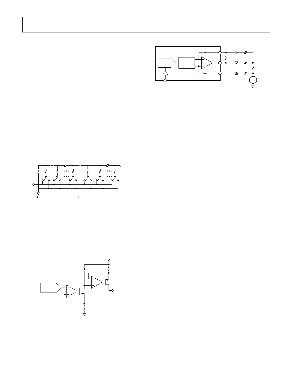
ARCHITECTURE
of two matched DAC sections. A simplified circuit diagram is
shown in Figure 65. The four MSBs of the 12-/16-bit data-word
are decoded to drive 15 switches, E1 to E15. Each of these switches
connects one of 15 matched resistors to either ground or the
reference buffer output. The remaining 8/12 bits of the data-
word drive the S0 to S7/S11 switches of an 8-/12-bit voltage
mode R-2R ladder network.
8-12 BIT R-2R LADDER
FOUR MSBs DECODED INTO
15 EQUAL SEGMENTS
2R
S0
S1
S7/S11
E1
E2
E15
VOUT
2R
06996-
057
Figure 65. DAC Ladder Structure
The voltage output from the DAC core is either converted to
a current (see Figure 66) which is then mirrored to the supply
rail so that the application simply sees a current source output
with respect to ground or it is buffered and scaled to output a
software selectable unipolar or bipolar voltage range (see
Figure 67). The current and voltage are output on separate
pins and cannot be output simultaneously.
12-/16-BIT
DAC
A1
AVDD
IOUT
A2
T1
T2
RSET
R2
R3
06996-
058
Figure 66. Voltage-to-Current Conversion Circuitry
06996-
059
12-/16-BIT
DAC
RANGE
SCALING
VCM
REFIN
+VSENSE
VOUT
–VSENSE
R1
RLOAD
–1V TO +3V
AD5412/AD5422
Figure 67. Voltage Output
Voltage Output Amplifier
The voltage output amplifier is capable of generating both
unipolar and bipolar output voltages. It is capable of driving
a load of 1 k in parallel with 1 F (with an external compen-
sation capacitor) to GND. The source and sink capabilities of
the output amplifier can be seen in Figure 37. The slew rate
is 1 V/s with a full-scale settling time of 25 s maximum (10 V
on top of a common-mode voltage (VCM) of 1 V to +3 V. In
output module applications where a cable could possibly
become disconnected from +VSENSE, resulting in the amplifier
loop being broken and possibly resulting in large destructive
voltages on VOUT, include an optional resistor (R1) between
2 kΩ and 5 kΩ to ensure the amplifier loop is kept closed. If
remote sensing of the load is not required, connect +VSENSE
directly to VOUT and connect VSENSE directly to GND. When
changing ranges on the voltage output, a glitch may occur. For
this reason, it is recommended that the output be disabled by
setting the OUTEN bit of the control register to logic low before
changing the output voltage range; this prevents a glitch from
occurring.
Driving Large Capacitive Loads
The voltage output amplifier is capable of driving capacitive
loads of up to 1 F with the addition of a nonpolarized 4 nF
compensation capacitor between the CCOMP and VOUT pins.
Without the compensation capacitor, up to 20 nF capacitive
loads can be driven.
相关PDF资料 |
PDF描述 |
|---|---|
| MS3454LS14S-2SX | CONN RCPT 4POS JAM NUT W/SCKT |
| ADV7123KSTZ140 | IC DAC VIDEO TRPL HI SPD 48-LQFP |
| AD7528JRZ | IC DAC 8BIT DUAL MULT 20-SOIC |
| VE-2NB-MW-F1 | CONVERTER MOD DC/DC 95V 100W |
| VI-B0X-MY-F3 | CONVERTER MOD DC/DC 5.2V 50W |
相关代理商/技术参数 |
参数描述 |
|---|---|
| AD5422AREZ-REEL | 功能描述:IC DAC 16BIT SRL 24TSSOP RoHS:是 类别:集成电路 (IC) >> 数据采集 - 数模转换器 系列:- 标准包装:47 系列:- 设置时间:2µs 位数:14 数据接口:并联 转换器数目:1 电压电源:单电源 功率耗散(最大):55µW 工作温度:-40°C ~ 85°C 安装类型:表面贴装 封装/外壳:28-SSOP(0.209",5.30mm 宽) 供应商设备封装:28-SSOP 包装:管件 输出数目和类型:1 电流,单极;1 电流,双极 采样率(每秒):* |
| AD5422BCPZ | 制造商:AD 制造商全称:Analog Devices 功能描述:Single Channel, 16-Bit, Serial Input, Current Source & Voltage Output DAC |
| AD5422BCPZ-REEL | 功能描述:IC DAC 16BIT SRL 40LFCSP RoHS:是 类别:集成电路 (IC) >> 数据采集 - 数模转换器 系列:- 标准包装:47 系列:- 设置时间:2µs 位数:14 数据接口:并联 转换器数目:1 电压电源:单电源 功率耗散(最大):55µW 工作温度:-40°C ~ 85°C 安装类型:表面贴装 封装/外壳:28-SSOP(0.209",5.30mm 宽) 供应商设备封装:28-SSOP 包装:管件 输出数目和类型:1 电流,单极;1 电流,双极 采样率(每秒):* |
| AD5422BCPZ-REEL7 | 功能描述:IC DAC 16BIT SRL 40LFCSP RoHS:是 类别:集成电路 (IC) >> 数据采集 - 数模转换器 系列:- 产品培训模块:Lead (SnPb) Finish for COTS Obsolescence Mitigation Program 标准包装:50 系列:- 设置时间:4µs 位数:12 数据接口:串行 转换器数目:2 电压电源:单电源 功率耗散(最大):- 工作温度:-40°C ~ 85°C 安装类型:表面贴装 封装/外壳:8-TSSOP,8-MSOP(0.118",3.00mm 宽) 供应商设备封装:8-uMAX 包装:管件 输出数目和类型:2 电压,单极 采样率(每秒):* 产品目录页面:1398 (CN2011-ZH PDF) |
| AD5422BREZ | 功能描述:IC DAC 16BIT 1CH 24TSSOP RoHS:是 类别:集成电路 (IC) >> 数据采集 - 数模转换器 系列:- 产品培训模块:Lead (SnPb) Finish for COTS Obsolescence Mitigation Program 标准包装:50 系列:- 设置时间:4µs 位数:12 数据接口:串行 转换器数目:2 电压电源:单电源 功率耗散(最大):- 工作温度:-40°C ~ 85°C 安装类型:表面贴装 封装/外壳:8-TSSOP,8-MSOP(0.118",3.00mm 宽) 供应商设备封装:8-uMAX 包装:管件 输出数目和类型:2 电压,单极 采样率(每秒):* 产品目录页面:1398 (CN2011-ZH PDF) |
发布紧急采购,3分钟左右您将得到回复。