参数资料
| 型号: | AD5425YRM |
| 厂商: | Analog Devices Inc |
| 文件页数: | 10/25页 |
| 文件大小: | 0K |
| 描述: | IC DAC MULTIPLYING 8BIT 10-MSOP |
| 产品培训模块: | Data Converter Fundamentals DAC Architectures |
| 标准包装: | 50 |
| 设置时间: | 15ns |
| 位数: | 8 |
| 数据接口: | 串行 |
| 转换器数目: | 1 |
| 电压电源: | 单电源 |
| 功率耗散(最大): | 25µW |
| 工作温度: | -40°C ~ 125°C |
| 安装类型: | 表面贴装 |
| 封装/外壳: | 10-TFSOP,10-MSOP(0.118",3.00mm 宽) |
| 供应商设备封装: | 10-MSOP |
| 包装: | 管件 |
| 输出数目和类型: | 2 电流,单极;2 电流,双极 |
| 采样率(每秒): | 9.5M |
| 配用: | EVAL-AD5425EBZ-ND - BOARD EVALUATION FOR AD5425 |
Data Sheet
AD5425
Rev. C | Page 17 of 24
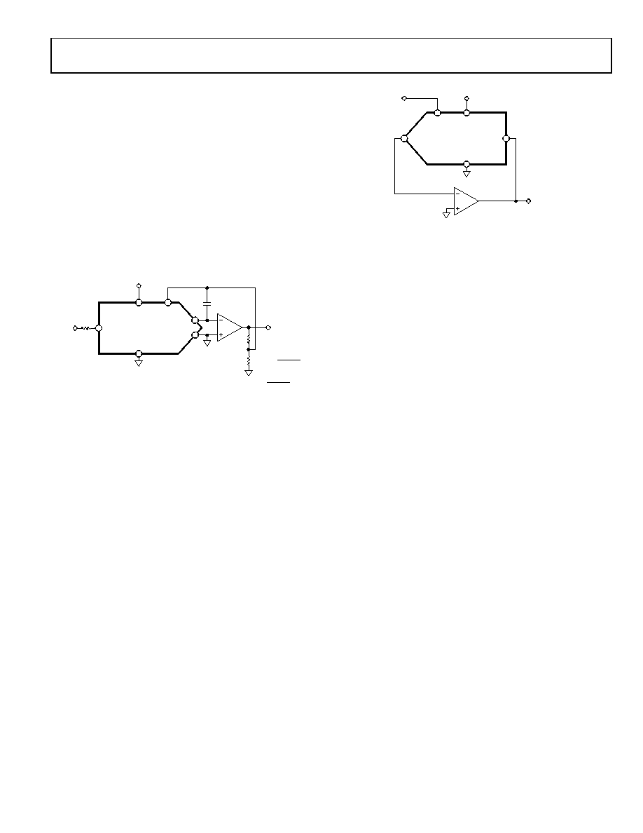
ADDING GAIN
In applications where the output voltage is required to be
greater than VIN, gain can be added with an additional external
amplifier or it can be achieved in a single stage. It is important
to take into consideration the effect of temperature coefficients
of the thin film resistors of the DAC. Simply placing a resistor in
series with the RFB resistor causes mismatches in the temp-
erature coefficients and results in larger gain temperature
coefficient errors. Instead, the circuit of Figure 35 is a recom-
mended method of increasing the gain of the circuit. R1, R2,
and R3 should all have similar temperature coefficients, but
they need not match the temperature coefficients of the DAC.
This approach is recommended in circuits where gains of
greater than 1 are required.
Figure 35. Increasing the Gain of Current Output DAC
DACS USED AS A DIVIDER OR PROGRAMMABLE
GAIN ELEMENT
Current steering DACs are very flexible and lend themselves to
many different applications. If this type of DAC is connected as
the feedback element of an op amp and RFB is used as the input
resistor as shown in Figure 36, then the output voltage is
inversely proportional to the digital input fraction, D.
For D = 1 2n, the output voltage is
VOUT = VIN/D = VIN/(1 2n)
As D is reduced, the output voltage increases. For small values
of D, it is important to ensure that the amplifier does not satur-
ate and that the required accuracy is met. For example, an 8-bit
DAC driven with the Binary Code 0x10 (00010000), that is,
16 decimal, in the circuit of Figure 36, should cause the output
voltage to be 16 × VIN. However, if the DAC has a linearity
specification of ±0.5 LSB, then D can in fact have a weight
anywhere in the range 15.5/256 to 16.5/256. Therefore, the
possible output voltage is in the range of 15.5 VIN to 16.5 VIN—
an error of 3%, even though the DAC itself has a maximum
error of 0.2%.
Figure 36. Current Steering DAC Used as a Divider or
Programmable Gain Element
DAC leakage current is also a potential error source in divider
circuits. The leakage current must be counterbalanced by an
opposite current supplied from the op amp through the DAC.
Since only a fraction, D, of the current into the VREF terminal is
routed to the IOUT1 terminal, the output voltage has to change
as follows:
Output Error Voltage Due to DAC Leakage = (Leakage × R)/D
where R is the DAC resistance at the VREF terminal. For a DAC
leakage current of 10 nA, R = 10 k. With a gain (that is, 1/D)
of 16 the error voltage is 1.6 mV.
REFERENCE SELECTION
When selecting a reference for use with the AD5425 current
output DAC, pay attention to the reference’s output voltage
temperature coefficient specification. This parameter not only
affects the full-scale error, but can also affect the linearity (INL
and DNL) performance. The reference temperature coefficient
should be consistent with the system accuracy specifications.
For example, an 8-bit system required to hold its overall
specification to within 1 LSB over the temperature range 0°C to
50°C dictates that the maximum system drift with temperature
should be less than 78 ppm/°C. A 12-bit system with the same
temperature range to overall specification within 2 LSB requires
a maximum drift of 10 ppm/°C. By choosing a precision
reference with a low output temperature coefficient, this error
source can be minimized. Table 7 suggests some of the
references available from Analog Devices that are suitable for
use with this range of current output DACs.
R1
R3
R2
VIN
R1 = R2R3
R2 + R3
GAIN = R2 + R3
R2
NOTES:
1. ADDITIONAL PINS OMITTED FOR CLARITY.
2. C1 PHASE COMPENSATION (1pF TO 2pF) MAY BE REQUIRED
IF A1 IS A HIGH SPEED AMPLIFIER.
VOUT
GND
IOUT2
IOUT1
RFB
A1
VREF
VDD
C1
03161-035
GND
IOUT1
RFB
VREF
VDD
NOTE:
1. ADDITIONAL PINS OMITTED FOR CLARITY.
VOUT
VIN
03161-036
相关PDF资料 |
PDF描述 |
|---|---|
| AD5443YRM | IC DAC 12BIT SERIAL IOUT 10-MSOP |
| AD5449YRU | IC DAC DUAL 12BIT MULT 16-TSSOP |
| AD5501BRUZ | IC DAC 12BIT SPI 16-TSSOP |
| AD5520JSTZ | IC PPMU SNGL-CH 64-LQFP |
| AD5522JSVUZ | IC PMU QUAD 16BIT DAC 80-TQFP |
相关代理商/技术参数 |
参数描述 |
|---|---|
| AD5425YRM-REEL | 功能描述:IC DAC 8BIT MULTIPLYING 10-MSOP RoHS:否 类别:集成电路 (IC) >> 数据采集 - 数模转换器 系列:- 产品培训模块:Data Converter Fundamentals DAC Architectures 设计资源:Unipolar, Precision DC Digital-to-Analog Conversion using AD5450/1/2/3 8-14-Bit DACs (CN0052) Precision, Bipolar, Configuration for AD5450/1/2/3 8-14bit Multiplying DACs (CN0053) AC Signal Processing Using AD5450/1/2/3 Current Output DACs (CN0054) Programmable Gain Element Using AD5450/1/2/3 Current Output DAC Family (CN0055) Single Supply Low Noise LED Current Source Driver Using a Current Output DAC in the Reverse Mode (CN0139) 标准包装:10,000 系列:- 设置时间:- 位数:12 数据接口:DSP,MICROWIRE?,QSPI?,串行,SPI? 转换器数目:1 电压电源:单电源 功率耗散(最大):- 工作温度:-40°C ~ 125°C 安装类型:表面贴装 封装/外壳:SOT-23-8 薄型,TSOT-23-8 供应商设备封装:TSOT-23-8 包装:带卷 (TR) 输出数目和类型:1 电流,单极;1 电流,双极 采样率(每秒):2.7M |
| AD5425YRM-REEL7 | 功能描述:IC DAC 8BIT MULTIPLYING 10-MSOP RoHS:否 类别:集成电路 (IC) >> 数据采集 - 数模转换器 系列:- 产品培训模块:Data Converter Fundamentals DAC Architectures 设计资源:Unipolar, Precision DC Digital-to-Analog Conversion using AD5450/1/2/3 8-14-Bit DACs (CN0052) Precision, Bipolar, Configuration for AD5450/1/2/3 8-14bit Multiplying DACs (CN0053) AC Signal Processing Using AD5450/1/2/3 Current Output DACs (CN0054) Programmable Gain Element Using AD5450/1/2/3 Current Output DAC Family (CN0055) Single Supply Low Noise LED Current Source Driver Using a Current Output DAC in the Reverse Mode (CN0139) 标准包装:10,000 系列:- 设置时间:- 位数:12 数据接口:DSP,MICROWIRE?,QSPI?,串行,SPI? 转换器数目:1 电压电源:单电源 功率耗散(最大):- 工作温度:-40°C ~ 125°C 安装类型:表面贴装 封装/外壳:SOT-23-8 薄型,TSOT-23-8 供应商设备封装:TSOT-23-8 包装:带卷 (TR) 输出数目和类型:1 电流,单极;1 电流,双极 采样率(每秒):2.7M |
| AD5425YRMZ | 功能描述:IC DAC 8BIT MULTIPLYING 10MSOP RoHS:是 类别:集成电路 (IC) >> 数据采集 - 数模转换器 系列:- 标准包装:1 系列:- 设置时间:4.5µs 位数:12 数据接口:串行,SPI? 转换器数目:1 电压电源:单电源 功率耗散(最大):- 工作温度:-40°C ~ 125°C 安装类型:表面贴装 封装/外壳:8-SOIC(0.154",3.90mm 宽) 供应商设备封装:8-SOICN 包装:剪切带 (CT) 输出数目和类型:1 电压,单极;1 电压,双极 采样率(每秒):* 其它名称:MCP4921T-E/SNCTMCP4921T-E/SNRCTMCP4921T-E/SNRCT-ND |
| AD5425YRMZ-REEL | 功能描述:IC DAC 8BIT MULTIPLYING 10MSOP RoHS:是 类别:集成电路 (IC) >> 数据采集 - 数模转换器 系列:- 产品培训模块:Data Converter Fundamentals DAC Architectures 设计资源:Unipolar, Precision DC Digital-to-Analog Conversion using AD5450/1/2/3 8-14-Bit DACs (CN0052) Precision, Bipolar, Configuration for AD5450/1/2/3 8-14bit Multiplying DACs (CN0053) AC Signal Processing Using AD5450/1/2/3 Current Output DACs (CN0054) Programmable Gain Element Using AD5450/1/2/3 Current Output DAC Family (CN0055) Single Supply Low Noise LED Current Source Driver Using a Current Output DAC in the Reverse Mode (CN0139) 标准包装:10,000 系列:- 设置时间:- 位数:12 数据接口:DSP,MICROWIRE?,QSPI?,串行,SPI? 转换器数目:1 电压电源:单电源 功率耗散(最大):- 工作温度:-40°C ~ 125°C 安装类型:表面贴装 封装/外壳:SOT-23-8 薄型,TSOT-23-8 供应商设备封装:TSOT-23-8 包装:带卷 (TR) 输出数目和类型:1 电流,单极;1 电流,双极 采样率(每秒):2.7M |
| AD5425YRMZ-REEL7 | 功能描述:IC DAC 8BIT MULTIPLYING 10MSOP RoHS:是 类别:集成电路 (IC) >> 数据采集 - 数模转换器 系列:- 产品培训模块:Data Converter Fundamentals DAC Architectures 设计资源:Unipolar, Precision DC Digital-to-Analog Conversion using AD5450/1/2/3 8-14-Bit DACs (CN0052) Precision, Bipolar, Configuration for AD5450/1/2/3 8-14bit Multiplying DACs (CN0053) AC Signal Processing Using AD5450/1/2/3 Current Output DACs (CN0054) Programmable Gain Element Using AD5450/1/2/3 Current Output DAC Family (CN0055) Single Supply Low Noise LED Current Source Driver Using a Current Output DAC in the Reverse Mode (CN0139) 标准包装:10,000 系列:- 设置时间:- 位数:12 数据接口:DSP,MICROWIRE?,QSPI?,串行,SPI? 转换器数目:1 电压电源:单电源 功率耗散(最大):- 工作温度:-40°C ~ 125°C 安装类型:表面贴装 封装/外壳:SOT-23-8 薄型,TSOT-23-8 供应商设备封装:TSOT-23-8 包装:带卷 (TR) 输出数目和类型:1 电流,单极;1 电流,双极 采样率(每秒):2.7M |
发布紧急采购,3分钟左右您将得到回复。