参数资料
| 型号: | AD5443YRM |
| 厂商: | Analog Devices Inc |
| 文件页数: | 10/25页 |
| 文件大小: | 0K |
| 描述: | IC DAC 12BIT SERIAL IOUT 10-MSOP |
| 产品培训模块: | Data Converter Fundamentals DAC Architectures |
| 设计资源: | Unipolar, Precision DC Digital-to-Analog Conversion Using AD5426/32/43 8-Bit to12-Bit DACs (CN0034) Precision, Bipolar Configuration for the AD5426/32/43 8-Bit to12-Bit DACs (CN0036) AC Signal Processing Using AD5426/32/43 Current Output DACs (CN0037) Programmable Gain Element Using AD5426/32/43 Current Output DACs (CN0038) Single-Ended-to-Differential Converters for Voltage Output and Current Output DACs Using AD8042 (CN0143) |
| 标准包装: | 50 |
| 位数: | 12 |
| 数据接口: | 串行 |
| 转换器数目: | 1 |
| 电压电源: | 单电源 |
| 工作温度: | -40°C ~ 125°C |
| 安装类型: | 表面贴装 |
| 封装/外壳: | 10-TFSOP,10-MSOP(0.118",3.00mm 宽) |
| 供应商设备封装: | 10-MSOP |
| 包装: | 管件 |
| 输出数目和类型: | 2 电流,单极;2 电流,双极 |
| 采样率(每秒): | 2.5M |
| 配用: | EVAL-AD5443-DBRDZ-ND - BOARD EVAL CARD CLINUX/STAMP |
Data Sheet
AD5426/AD5432/AD5443
Rev. G | Page 17 of 24
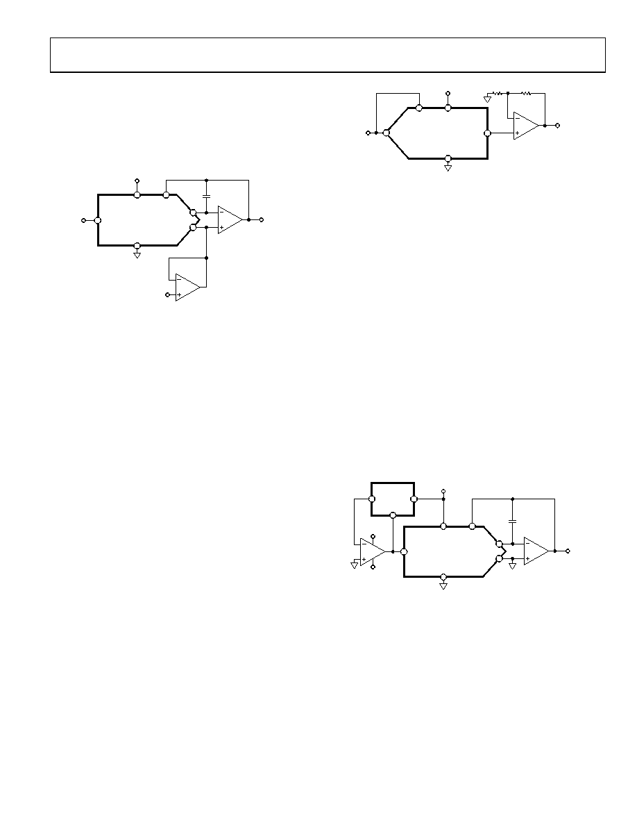
SINGLE-SUPPLY APPLICATIONS
Current Mode Operation
These DACs are specified and tested to guarantee operation
in single-supply applications. In the current mode circuit of
applied to VBIAS.
VOUT
GND
VIN
IOUT2
IOUT1
RFB
A1
VREF
VDD
VBIAS
VDD
C1
NOTES
1. ADDITIONAL PINS OMITTED FOR CLARITY.
2. C1 PHASE COMPENSATION (1pF TO 2pF) MAY BE
REQUIRED IF A1 IS A HIGH SPEED AMPLIFIER.
A1
03162-044
A2
Figure 43. Single-Supply Current Mode Operation
In this configuration, the output voltage is given by
VOUT = {D × (RFB/RDAC) × (VBIAS VIN)} + VBIAS
(AD5443), the output voltage varies from
VOUT = VBIAS to VOUT = 2 VBIAS VIN
VBIAS should be a low impedance source capable of sinking and
sourcing all possible variations in current at the IOUT2 terminal
without any problems.
It is important to note that VIN is limited to low voltages because
the switches in the DAC ladder no longer have the same source
drain drive voltage. As a result, their on resistance differs, which
degrades the linearity of the DAC. See Figure 15 to Figure 20.
Voltage Switching Mode of Operation
Figure 44 shows these DACs operating in the voltage switching
mode. The reference voltage, VIN, is applied to the IOUT1 pin,
IOUT2 is connected to AGND, and the output voltage is available
at the VREF terminal. In this configuration, a positive reference
voltage results in a positive output voltage, making single-
supply operation possible. The output from the DAC is voltage
at a constant impedance (the DAC ladder resistance), thus an
op amp is necessary to buffer the output voltage. The reference
input no longer sees a constant input impedance, but one that
varies with code. Therefore, the voltage input should be driven
from a low impedance source.
VIN
R2
R1
VOUT
GND
IOUT1
RFB
A1
VREF
VDD
NOTES
1. ADDITIONAL PINS OMITTED FOR CLARITY.
2. C1 PHASE COMPENSATION (1pF TO 2pF) MAY BE REQUIRED
IF A1 IS A HIGH SPEED AMPLIFIER.
03162-045
Figure 44. Single-Supply Voltage Switching Mode Operation
It is important to note that VIN is limited to low voltages because
the switches in the DAC ladder no longer have the same source
drain drive voltage. As a result, their on resistance differs, which
degrades the linearity of the DAC.
Also, VIN must not go negative by more than 0.3 V or an
internal diode turns on, exceeding the maximum ratings of the
device. In this type of application, the full range of multiplying
capability of the DAC is lost.
POSITIVE OUTPUT VOLTAGE
Note that the output voltage polarity is opposite to the VREF
polarity for dc reference voltages. To achieve a positive voltage
output, an applied negative reference to the input of the DAC
is preferred over the output inversion through an inverting
amplifier because of the resistor’s tolerance errors. To generate
a negative reference, the reference can be level shifted by an
op amp such that the VOUT and GND pins of the reference
become the virtual ground and 2.5 V, respectively, as shown
NOTES
1. ADDITIONAL PINS OMITTED FOR CLARITY.
2. C1 PHASE COMPENSATION (1pF TO 2pF) MAY BE REQUIRED IF A1 IS
A HIGH SPEED AMPLIFIER.
VOUT = 0V
TO +2.5V
GND
IOUT2
IOUT1
RFB
A1
VREF
VDD = 5V
VDD
C1
GND
VIN
VOUT
ADR03
–2.5V
–5V
+5V
03162-046
Figure 45. Positive Voltage Output with Minimum of Components
相关PDF资料 |
PDF描述 |
|---|---|
| AD5449YRU | IC DAC DUAL 12BIT MULT 16-TSSOP |
| AD5501BRUZ | IC DAC 12BIT SPI 16-TSSOP |
| AD5520JSTZ | IC PPMU SNGL-CH 64-LQFP |
| AD5522JSVUZ | IC PMU QUAD 16BIT DAC 80-TQFP |
| AD5532ABC-5 | IC DAC 14BIT 32CH 74-CSPBGA |
相关代理商/技术参数 |
参数描述 |
|---|---|
| AD5443YRM-REEL | 制造商:Analog Devices 功能描述:DAC 1-CH R-2R 12-bit 10-Pin MSOP T/R 制造商:Analog Devices 功能描述:DAC 1CH R-2R 12-BIT 10MSOP - Tape and Reel 制造商:Rochester Electronics LLC 功能描述:12-BIT IOUT DAC WITH SERIAL ITF I.C. - Tape and Reel |
| AD5443YRM-REEL7 | 制造商:Analog Devices 功能描述:DAC 1-CH R-2R 12-bit 10-Pin MSOP T/R 制造商:Analog Devices 功能描述:DAC 1CH R-2R 12-BIT 10MSOP - Tape and Reel |
| AD5443YRMZ | 功能描述:IC DAC 12BIT SERIAL IOUT 10-MSOP RoHS:是 类别:集成电路 (IC) >> 数据采集 - 数模转换器 系列:- 产品培训模块:Lead (SnPb) Finish for COTS Obsolescence Mitigation Program 标准包装:50 系列:- 设置时间:4µs 位数:12 数据接口:串行 转换器数目:2 电压电源:单电源 功率耗散(最大):- 工作温度:-40°C ~ 85°C 安装类型:表面贴装 封装/外壳:8-TSSOP,8-MSOP(0.118",3.00mm 宽) 供应商设备封装:8-uMAX 包装:管件 输出数目和类型:2 电压,单极 采样率(每秒):* 产品目录页面:1398 (CN2011-ZH PDF) |
| AD5443YRMZ | 制造商:Analog Devices 功能描述:IC 12BIT DAC SERIAL I/F SMD 5443 |
| AD5443YRMZ-REEL | 功能描述:IC DAC 12BIT SERIAL IN 10MSOP RoHS:是 类别:集成电路 (IC) >> 数据采集 - 数模转换器 系列:- 产品培训模块:LTC263x 12-, 10-, and 8-Bit VOUT DAC Family 特色产品:LTC2636 - Octal 12-/10-/8-Bit SPI VOUT DACs with 10ppm/°C Reference 标准包装:91 系列:- 设置时间:4µs 位数:10 数据接口:MICROWIRE?,串行,SPI? 转换器数目:8 电压电源:单电源 功率耗散(最大):2.7mW 工作温度:-40°C ~ 85°C 安装类型:表面贴装 封装/外壳:14-WFDFN 裸露焊盘 供应商设备封装:14-DFN-EP(4x3) 包装:管件 输出数目和类型:8 电压,单极 采样率(每秒):* |
发布紧急采购,3分钟左右您将得到回复。