- 您现在的位置:买卖IC网 > PDF目录8709 > AD5444YRM-REEL7 (Analog Devices Inc)IC DAC 12BIT MULTIPLYING 10-MSOP PDF资料下载
参数资料
| 型号: | AD5444YRM-REEL7 |
| 厂商: | Analog Devices Inc |
| 文件页数: | 14/29页 |
| 文件大小: | 0K |
| 描述: | IC DAC 12BIT MULTIPLYING 10-MSOP |
| 产品培训模块: | Data Converter Fundamentals DAC Architectures |
| 标准包装: | 1,000 |
| 设置时间: | 16ns |
| 位数: | 12 |
| 数据接口: | 串行 |
| 转换器数目: | 1 |
| 电压电源: | 单电源 |
| 功率耗散(最大): | 50.5µW |
| 工作温度: | -40°C ~ 125°C |
| 安装类型: | 表面贴装 |
| 封装/外壳: | 10-TFSOP,10-MSOP(0.118",3.00mm 宽) |
| 供应商设备封装: | 10-MSOP |
| 包装: | 带卷 (TR) |
| 输出数目和类型: | 2 电流,单极;2 电流,双极 |
| 采样率(每秒): | 2.7M |
第1页第2页第3页第4页第5页第6页第7页第8页第9页第10页第11页第12页第13页当前第14页第15页第16页第17页第18页第19页第20页第21页第22页第23页第24页第25页第26页第27页第28页第29页
AD5444/AD5446
Data Sheet
Rev. E | Page 20 of 28
SERIAL INTERFACE
The AD5444/AD5446 have an easy-to-use, 3-wire interface that
is compatible with SPI, QSPI, MICROWIRE, and DSP inter-
face standards. Data is written to the device in 16-bit words.
This 16-bit word consists of two control bits, 12 data bits or
14 data bits, as shown in Figure 44 and Figure 45. The AD5446
uses all 14 bits of DAC data while AD5444 uses 12 bits and
ignores the 2 LSBs.
Control Bit C1 and Control Bit C0 allow the user to load and
update the new DAC code and to change the active clock edge.
By default, the shift register clocks data on the falling edge, but
this can be changed via the control bits. If changed, the DAC
core is inoperative until the next data frame. A power cycle
resets this back to the default condition. On-chip, power-on
reset circuitry ensures the device powers on with zero scale
loaded to the DAC register and the IOUT line.
Table 10. DAC Control Bits
C1
C0
Function Implemented
0
Load and update (power-on default)
0
1
Disable SDO
1
0
No operation
1
Clock data to shift register on rising edge
SYNC Function
SYNC is an edge-triggered input that acts as a frame synchroni-
zation signal. Data can be transferred into the device only while
SYNC is low. To start the serial data transfer, SYNC should be
taken low, observing the minimum SYNC falling to the SCLK
falling edge setup time, t4. To minimize the power consumption
of the device, the interface powers up fully only when the device
is being written to, that is, on the falling edge of SYNC.
The SCLK and DIN input buffers are powered down on the
rising edge of SYNC.
After the falling edge of the 16th SCLK pulse, bring SYNC high
to transfer data from the input shift register to the DAC register.
Daisy-Chain Mode
Daisy-chain mode is the default power-on mode. To disable
the daisy-chain function, write 01 to the control word. In daisy-
chain mode, the internal gating on the SCLK is disabled. The
SCLK is continuously applied to the input shift register when
SYNC is low. If more than 16 clock pulses are applied, the data
ripples out of the shift register and appears on the SDO line.
This data is clocked out on the rising edge of the SCLK (this
is the default; use the control word to change the active edge)
and is valid for the next device on the falling edge (default).
By connecting this line to the SDIN input on the next device in
the chain, a multidevice interface is constructed. Sixteen clock
pulses are required for each device in the system. Therefore, the
total number of clock cycles must equal 16 N, where N is the
number of devices in the chain.
When the serial transfer to all devices is complete, SYNC
should be taken high. This prevents any further data from
being clocked into the shift register. A burst clock containing
the exact number of clock cycles can be used, and SYNC can be
taken high some time later. After the rising edge of SYNC, data
is automatically transferred from each device’s input register to
the addressed DAC.
When the control bits = 10, the device is in no operation mode.
This can be useful in daisy-chain applications where the user
does not want to change the settings of a particular DAC in the
chain. Simply write 10 to the control bits for that DAC and the
following data bits are ignored.
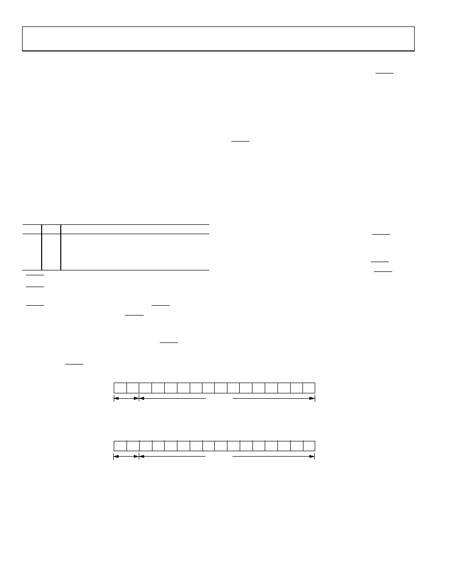
04588-
037
DB0 (LSB)
DB15 (MSB)
DB7 DB6 DB5 DB4
DB3 DB2
DB0
DB1
C1
C0
DB11 DB10
DB8
DB9
X
CONTROL BITS
DATA BITS
Figure 44. AD5444 12-Bit Input Shift Register Contents
04588-
038
DB0 (LSB)
DB15 (MSB)
DB9 DB8 DB7
DB6 DB5 DB4
DB2
DB3
C1
C0
DB13 DB12
DB10
DB11
DB0
DB1
CONTROL BITS
DATA BITS
Figure 45. AD5446 14-Bit Input Shift Register Contents
相关PDF资料 |
PDF描述 |
|---|---|
| AD5647RBRMZ-REEL7 | IC DAC NANO 14BIT DUAL 10-MSOP |
| LTC1426CS8#TR | IC DAC PWM 6BIT DUAL MCPWR 8SOIC |
| AD5341BRUZ-REEL7 | IC DAC 12BIT SNGL VOUT 20-TSSOP |
| SL23EP08SC-4 | IC BUFFER 220MHZ 8CH 3.3V 16SOIC |
| SL23EP08SC-4H | IC BUFFER 220MHZ 8CH3.3V 16TSOIC |
相关代理商/技术参数 |
参数描述 |
|---|---|
| AD5444YRMZ | 功能描述:IC DAC 12BIT SERIAL OUT 10MSOP RoHS:是 类别:集成电路 (IC) >> 数据采集 - 数模转换器 系列:- 产品培训模块:Lead (SnPb) Finish for COTS Obsolescence Mitigation Program 标准包装:50 系列:- 设置时间:4µs 位数:12 数据接口:串行 转换器数目:2 电压电源:单电源 功率耗散(最大):- 工作温度:-40°C ~ 85°C 安装类型:表面贴装 封装/外壳:8-TSSOP,8-MSOP(0.118",3.00mm 宽) 供应商设备封装:8-uMAX 包装:管件 输出数目和类型:2 电压,单极 采样率(每秒):* 产品目录页面:1398 (CN2011-ZH PDF) |
| AD5444YRMZ-REEL | 功能描述:IC DAC 12BIT MULTIPLYING 10-MSOP RoHS:是 类别:集成电路 (IC) >> 数据采集 - 数模转换器 系列:- 产品培训模块:LTC263x 12-, 10-, and 8-Bit VOUT DAC Family 特色产品:LTC2636 - Octal 12-/10-/8-Bit SPI VOUT DACs with 10ppm/°C Reference 标准包装:91 系列:- 设置时间:4µs 位数:10 数据接口:MICROWIRE?,串行,SPI? 转换器数目:8 电压电源:单电源 功率耗散(最大):2.7mW 工作温度:-40°C ~ 85°C 安装类型:表面贴装 封装/外壳:14-WFDFN 裸露焊盘 供应商设备封装:14-DFN-EP(4x3) 包装:管件 输出数目和类型:8 电压,单极 采样率(每秒):* |
| AD5444YRMZ-REEL7 | 功能描述:IC DAC 12BIT MULTIPLYING 10-MSOP RoHS:是 类别:集成电路 (IC) >> 数据采集 - 数模转换器 系列:- 产品培训模块:LTC263x 12-, 10-, and 8-Bit VOUT DAC Family 特色产品:LTC2636 - Octal 12-/10-/8-Bit SPI VOUT DACs with 10ppm/°C Reference 标准包装:91 系列:- 设置时间:4µs 位数:10 数据接口:MICROWIRE?,串行,SPI? 转换器数目:8 电压电源:单电源 功率耗散(最大):2.7mW 工作温度:-40°C ~ 85°C 安装类型:表面贴装 封装/外壳:14-WFDFN 裸露焊盘 供应商设备封装:14-DFN-EP(4x3) 包装:管件 输出数目和类型:8 电压,单极 采样率(每秒):* |
| AD5445 | 制造商:AD 制造商全称:Analog Devices 功能描述:Dual 8-,10-,12-Bit High Bandwidth Multiplying DACs with Serial Interface |
| AD5445YCP | 制造商:Analog Devices 功能描述:DAC 1-CH R-2R 12-bit 20-Pin LFCSP EP 制造商:Rochester Electronics LLC 功能描述:12-BIT LOUT DAC PARELLED INT/FACE I.C. - Bulk 制造商:Analog Devices 功能描述:12BIT DAC PARALLEL I/F SMD 5445 |
发布紧急采购,3分钟左右您将得到回复。