参数资料
| 型号: | AD5447YRUZ |
| 厂商: | Analog Devices Inc |
| 文件页数: | 13/33页 |
| 文件大小: | 0K |
| 描述: | IC DAC 12BIT DUAL MULT 24-TSSOP |
| 产品培训模块: | Data Converter Fundamentals DAC Architectures |
| 标准包装: | 62 |
| 设置时间: | 80ns |
| 位数: | 12 |
| 数据接口: | 并联 |
| 转换器数目: | 2 |
| 电压电源: | 单电源 |
| 功率耗散(最大): | 3.3µW |
| 工作温度: | -40°C ~ 125°C |
| 安装类型: | 表面贴装 |
| 封装/外壳: | 24-TSSOP(0.173",4.40mm 宽) |
| 供应商设备封装: | 24-TSSOP |
| 包装: | 管件 |
| 输出数目和类型: | 2 电流,单极;2 电流,双极 |
| 采样率(每秒): | 21.3M |
| 产品目录页面: | 782 (CN2011-ZH PDF) |
| 配用: | EVAL-AD5447EBZ-ND - BOARD EVALUATION FOR AD5447 |
第1页第2页第3页第4页第5页第6页第7页第8页第9页第10页第11页第12页当前第13页第14页第15页第16页第17页第18页第19页第20页第21页第22页第23页第24页第25页第26页第27页第28页第29页第30页第31页第32页第33页
Data Sheet
AD5428/AD5440/AD5447
Rev. C | Page 19 of 32
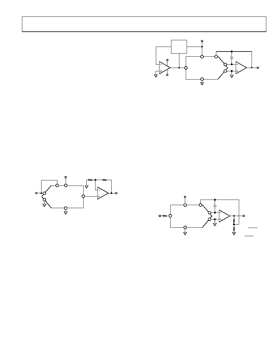
SINGLE-SUPPLY APPLICATIONS
Voltage-Switching Mode
Figure 40 shows the DACs operating in voltage-switching
mode. The reference voltage, VIN, is applied to the IOUTA pin,
and the output voltage is available at the VREFA terminal. In this
configuration, a positive reference voltage results in a positive
output voltage, making single-supply operation possible. The
output from the DAC is voltage at constant impedance (the
DAC ladder resistance). Therefore, an op amp is necessary to
buffer the output voltage. The reference input no longer sees
constant input impedance, but one that varies with code.
Therefore, the voltage input should be driven from a low
impedance source.
Note that VIN is limited to low voltages because the switches in
the DAC ladder no longer have the same source-drain drive
voltage. As a result, their on resistance differs and degrades the
integral linearity of the DAC. Also, VIN must not go negative by
more than 0.3 V, or an internal diode turns on, causing the
device to exceed the maximum ratings. In this type of
application, the full range of multiplying capability of the DAC
is lost.
04462-033
NOTES
1. ADDITIONAL PINS OMITTED FOR CLARITY.
2. C1 PHASE COMPENSATION (1pF TO 2pF) MAY BE REQUIRED
IF A1 IS A HIGH SPEED AMPLIFIER.
VDD
VIN
VREFA
VDD
RFBA
GND
VOUT
IOUTA
AGND
R1
R2
Figure 40. Single-Supply Voltage-Switching Mode
Positive Output Voltage
The output voltage polarity is opposite to the VREF polarity for
dc reference voltages. To achieve a positive voltage output, an
applied negative reference to the input of the DAC is preferred
over the output inversion through an inverting amplifier
because of the resistor’s tolerance errors. To generate a negative
reference, the reference can be level-shifted by an op amp such
that the VOUT and GND pins of the reference become the virtual
ground and –2.5 V, respectively, as shown in Figure 41.
04462-034
NOTES
1. ADDITIONAL PINS OMITTED FOR CLARITY.
2. C1 PHASE COMPENSATION (1pF TO 2pF) MAY BE REQUIRED
IF A1 IS A HIGH SPEED AMPLIFIER.
VDD = 5V
VDD
C1
VIN
VREFA
RFBA
8-/10-/12-BIT
DAC
ADR03
GND
VOUT
VOUT =
0V to 2.5V
IOUTA
AGND
+5V
–5V
–2.5V
Figure 41. Positive Voltage Output with Minimum Components
ADDING GAIN
In applications where the output voltage must be greater than
VIN, gain can be added with an additional external amplifier, or
it can be achieved in a single stage. Consider the effect of temper-
ature coefficients of the thin film resistors of the DAC. Simply
placing a resistor in series with the RFB resistor causes mismatches
in the temperature coefficients, resulting in larger gain temper-
ature coefficient errors. Instead, the circuit in Figure 42 shows
the recommended method for increasing the gain of the circuit.
R1, R2, and R3 should have similar temperature coefficients,
but they need not match the temperature coefficients of the
DAC. This approach is recommended in circuits where gains of
greater than 1 are required.
04462-035
NOTES
1. ADDITIONAL PINS OMITTED FOR CLARITY.
2. C1 PHASE COMPENSATION (1pF TO 2pF) MAY BE REQUIRED
IF A1 IS A HIGH SPEED AMPLIFIER.
VDD
C1
VIN
VREFA
RFBA
R1
R3
R2
8-/10-/12-BIT
DAC
GND
VOUT
IOUTA
AGND
R2 + R3
R2
GAIN =
R1 =
R2R3
R2 + R3
Figure 42. Increasing Gain of Current Output DAC
相关PDF资料 |
PDF描述 |
|---|---|
| MS3127E16-8S | CONN RCPT 8POS BOX MNT W/SCKT |
| MS27474P24A35S | CONN RCPT 128POS JAM NUT W/SCKT |
| MS27497T24F2SD | CONN RCPT 100POS WALL MNT W/SCKT |
| VI-BNK-MV-F4 | CONVERTER MOD DC/DC 40V 150W |
| ICS843253AGI-45LFT | IC SYNTHESIZER LVPECL 16-TSSOP |
相关代理商/技术参数 |
参数描述 |
|---|---|
| AD5447YRUZ-REEL | 功能描述:IC DAC 12BIT DUAL MULT 24TSSOP RoHS:是 类别:集成电路 (IC) >> 数据采集 - 数模转换器 系列:- 产品培训模块:LTC263x 12-, 10-, and 8-Bit VOUT DAC Family 特色产品:LTC2636 - Octal 12-/10-/8-Bit SPI VOUT DACs with 10ppm/°C Reference 标准包装:91 系列:- 设置时间:4µs 位数:10 数据接口:MICROWIRE?,串行,SPI? 转换器数目:8 电压电源:单电源 功率耗散(最大):2.7mW 工作温度:-40°C ~ 85°C 安装类型:表面贴装 封装/外壳:14-WFDFN 裸露焊盘 供应商设备封装:14-DFN-EP(4x3) 包装:管件 输出数目和类型:8 电压,单极 采样率(每秒):* |
| AD5447YRUZ-REEL7 | 功能描述:IC DAC 12BIT DUAL MULT 24TSSOP RoHS:是 类别:集成电路 (IC) >> 数据采集 - 数模转换器 系列:- 产品培训模块:LTC263x 12-, 10-, and 8-Bit VOUT DAC Family 特色产品:LTC2636 - Octal 12-/10-/8-Bit SPI VOUT DACs with 10ppm/°C Reference 标准包装:91 系列:- 设置时间:4µs 位数:10 数据接口:MICROWIRE?,串行,SPI? 转换器数目:8 电压电源:单电源 功率耗散(最大):2.7mW 工作温度:-40°C ~ 85°C 安装类型:表面贴装 封装/外壳:14-WFDFN 裸露焊盘 供应商设备封装:14-DFN-EP(4x3) 包装:管件 输出数目和类型:8 电压,单极 采样率(每秒):* |
| AD5449 | 制造商:AD 制造商全称:Analog Devices 功能描述:Dual 8-,10-,12-Bit High Bandwidth Multiplying DACs with Serial Interface |
| AD5449YRU | 功能描述:IC DAC DUAL 12BIT MULT 16-TSSOP RoHS:否 类别:集成电路 (IC) >> 数据采集 - 数模转换器 系列:- 标准包装:47 系列:- 设置时间:2µs 位数:14 数据接口:并联 转换器数目:1 电压电源:单电源 功率耗散(最大):55µW 工作温度:-40°C ~ 85°C 安装类型:表面贴装 封装/外壳:28-SSOP(0.209",5.30mm 宽) 供应商设备封装:28-SSOP 包装:管件 输出数目和类型:1 电流,单极;1 电流,双极 采样率(每秒):* |
| AD5449YRU-REEL | 功能描述:IC DAC DUAL 12BIT MULT 16-TSSOP RoHS:否 类别:集成电路 (IC) >> 数据采集 - 数模转换器 系列:- 产品培训模块:LTC263x 12-, 10-, and 8-Bit VOUT DAC Family 特色产品:LTC2636 - Octal 12-/10-/8-Bit SPI VOUT DACs with 10ppm/°C Reference 标准包装:91 系列:- 设置时间:4µs 位数:10 数据接口:MICROWIRE?,串行,SPI? 转换器数目:8 电压电源:单电源 功率耗散(最大):2.7mW 工作温度:-40°C ~ 85°C 安装类型:表面贴装 封装/外壳:14-WFDFN 裸露焊盘 供应商设备封装:14-DFN-EP(4x3) 包装:管件 输出数目和类型:8 电压,单极 采样率(每秒):* |
发布紧急采购,3分钟左右您将得到回复。