- 您现在的位置:买卖IC网 > PDF目录9015 > AD5450YUJZ-REEL7 (Analog Devices Inc)IC DAC 8BIT MULT 50MHZ TSOT23-8 PDF资料下载
参数资料
| 型号: | AD5450YUJZ-REEL7 |
| 厂商: | Analog Devices Inc |
| 文件页数: | 15/28页 |
| 文件大小: | 0K |
| 描述: | IC DAC 8BIT MULT 50MHZ TSOT23-8 |
| 产品培训模块: | Data Converter Fundamentals DAC Architectures |
| 设计资源: | Unipolar, Precision DC Digital-to-Analog Conversion using AD5450/1/2/3 8-14-Bit DACs (CN0052) Precision, Bipolar, Configuration for AD5450/1/2/3 8-14bit Multiplying DACs (CN0053) AC Signal Processing Using AD5450/1/2/3 Current Output DACs (CN0054) Programmable Gain Element Using AD5450/1/2/3 Current Output DAC Family (CN0055) |
| 标准包装: | 1 |
| 位数: | 8 |
| 数据接口: | DSP,MICROWIRE?,QSPI?,串行,SPI? |
| 转换器数目: | 1 |
| 电压电源: | 单电源 |
| 工作温度: | -40°C ~ 125°C |
| 安装类型: | 表面贴装 |
| 封装/外壳: | SOT-23-8 薄型,TSOT-23-8 |
| 供应商设备封装: | TSOT-23-8 |
| 包装: | 标准包装 |
| 输出数目和类型: | 1 电流,单极;1 电流,双极 |
| 采样率(每秒): | 2.7M |
| 产品目录页面: | 782 (CN2011-ZH PDF) |
| 其它名称: | AD5450YUJZ-REEL7DKR |
第1页第2页第3页第4页第5页第6页第7页第8页第9页第10页第11页第12页第13页第14页当前第15页第16页第17页第18页第19页第20页第21页第22页第23页第24页第25页第26页第27页第28页
AD5450/AD5451/AD5452/AD5453
Data Sheet
Rev. G | Page 22 of 28
04
58
7-
0
5
10
0
00
0
11
0
CONTROL BITS
DATA BITS
10
0
00
0
00
11
0
CONTROL BITS
ACTUAL DATA FRAME
INTENDED DATA FRAME
DATA BITS
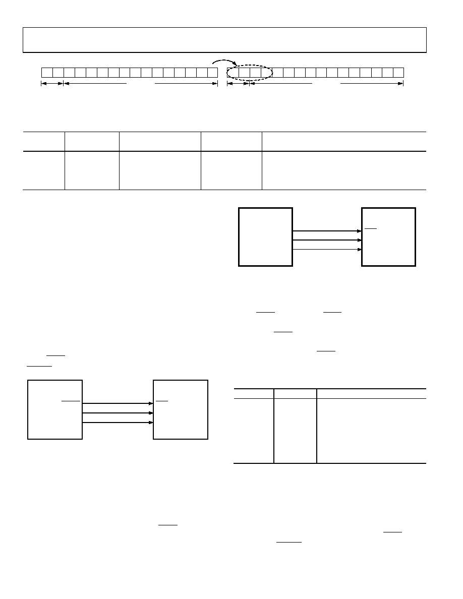
Figure 55. AD5453 Second Write, Incomplete Data Sequence (0x3200) and Subsequent Additional Bits (0xF200)
Table 11.
Writing
Sequence
Data Write in
Shift Register
Action Expected
Data Transfer to
the Device
Action Carried Out
1
0x3FFF
Load and update 0x3FFF
0x3FFF
Load and update 0x3FFF
2
0x3200
Load and update 0x3200
0xF200
Clock data to shift register upon rising edge (0xF200)
MICROPROCESSOR INTERFACING
/AD5453 DAC is through a serial bus that uses standard protocol
and is compatible with microcontrollers and DSP processors.
The communication channel is a 3-wire interface consisting of
a clock signal, a data signal, and a synchronization signal. The
the default being data valid upon the falling edge of SCLK, but
this is changeable using the control bits in the data-word.
ADSP-21xx-to-AD5450/AD5451/AD5452/AD5453
Interface
The ADSP-21xx family of DSPs is easily interfaced to a AD5450/
logic. Figure 56 is an example of an SPI interface between the DAC
and the ADSP-2191M. SCK of the DSP drives the serial data line,
SDIN. SYNC is driven from one of the port lines, in this case
SPIxSEL.
SCLK
SCK
SYNC
SPIxSEL
SDIN
MOSI
ADSP-2191M*
*ADDITIONAL PINS OMITTED FOR CLARITY
AD5450/AD5451/
AD5452/AD5453*
0
458
7-
1
00
A serial interface between the DAC and DSP SPORT is shown
in Figure 57. In this example, SPORT0 is used to transfer data to
the DAC shift register. Transmission is initiated by writing a
word to the Tx register after the SPORT has been enabled. In a
write sequence, data is clocked out upon each rising edge of the
DSP’s serial clock and clocked into the DAC input shift register
upon the falling edge of its SCLK. The update of the DAC
output takes place upon the rising edge of the SYNC signal.
SCLK
SYNC
TFS
SDIN
DT
ADSP-2101/
ADSP-2191M*
*ADDITIONAL PINS OMITTED FOR CLARITY
0
4587-
051
AD5450/AD5451/
AD5452/AD5453*
Figure 57. ADSP-2101/ADSP-2191M-
Communication between two devices at a given clock speed is
possible when the following specifications are compatible:
frame SYNC delay and frame SYNC setup-and-hold, data delay
and data setup-and-hold, and SCLK width. The DAC interface
expects a t4 (SYNC falling edge to SCLK falling edge setup time)
of 13 ns minimum. See the ADSP-21xx User Manual for infor-
mation on clock and frame SYNC frequencies for the SPORT
register. Table 12 shows the setup for the SPORT control register.
Table 12. SPORT Control Register Setup
Name
Setting
Description
TFSW
1
Alternate framing
INVTFS
1
Active low frame signal
DTYPE
00
Right justify data
ISCLK
1
Internal serial clock
TFSR
1
Frame every word
ITFS
1
Internal framing signal
SLEN
1111
16-bit data-word
ADSP-BF5xx-to-AD5450/AD5451/AD5452/AD5453
Interface
The ADSP-BF5xx family of processors has an SPI-compatible
port that enables the processor to communicate with SPI-
compatible devices. A serial interface between the BlackFin
shown in Figure 58. In this configuration, data is transferred
through the MOSI (master output, slave input) pin. SYNC is
driven by the SPIxSEL pin, which is a reconfigured
programmable flag pin.
相关PDF资料 |
PDF描述 |
|---|---|
| VI-J7K-MZ-F3 | CONVERTER MOD DC/DC 40V 25W |
| ICS601R-25LFT | IC CLOCK MULTIPLIER 1:5 20-SSOP |
| ICS601G-21LFT | IC CLOCK MULTIPLIER 16-TSSOP |
| ICS525R-03ILFT | IC CLOCK USER CONFIG 28-SSOP |
| ICS843SDNAGLFT | IC GENERATOR FEMTOCLOCK 8TSSOP |
相关代理商/技术参数 |
参数描述 |
|---|---|
| AD5451 | 制造商:AD 制造商全称:Analog Devices 功能描述:Dual 8-,10-,12-Bit High Bandwidth Multiplying DACs with Serial Interface |
| AD5451YUJ | 制造商:Analog Devices 功能描述:DAC 1CH R-2R 10-BIT 8PIN TSOT - Bulk |
| AD5451YUJ-REEL | 制造商:Analog Devices 功能描述:DAC 1-CH Segment 10-bit 8-Pin TSOT T/R |
| AD5451YUJ-REEL7 | 制造商:Analog Devices 功能描述:DAC 1-CH Segment 10-bit 8-Pin TSOT T/R 制造商:Rochester Electronics LLC 功能描述: |
| AD5451YUJZ | 制造商:Analog Devices 功能描述:IC,CMOS 10-bit DAC,AD5451YUJZ |
发布紧急采购,3分钟左右您将得到回复。