- 您现在的位置:买卖IC网 > PDF目录8645 > AD5531BRUZ-REEL (Analog Devices Inc)IC DAC 14BIT SRL IN/VOUT 16TSSOP PDF资料下载
参数资料
| 型号: | AD5531BRUZ-REEL |
| 厂商: | Analog Devices Inc |
| 文件页数: | 7/20页 |
| 文件大小: | 0K |
| 描述: | IC DAC 14BIT SRL IN/VOUT 16TSSOP |
| 产品培训模块: | Data Converter Fundamentals DAC Architectures |
| 标准包装: | 2,500 |
| 设置时间: | 20µs |
| 位数: | 14 |
| 数据接口: | 串行 |
| 转换器数目: | 1 |
| 电压电源: | 模拟和数字 |
| 功率耗散(最大): | 60mW |
| 工作温度: | -40°C ~ 85°C |
| 安装类型: | 表面贴装 |
| 封装/外壳: | 16-TSSOP(0.173",4.40mm 宽) |
| 供应商设备封装: | 16-TSSOP |
| 包装: | 带卷 (TR) |
| 输出数目和类型: | 1 电压,双极 |
| 采样率(每秒): | 50k |
AD5530/AD5531
Rev. B | Page 15 of 20
MICROPROCESSOR INTERFACING
Microprocessor interfacing to the AD5530/AD5531 is via a
serial bus that uses standard protocol compatible with micro-
controllers and DSP processors. The communications channel
is a 3-wire (minimum) interface consisting of a clock signal, a
data signal, and a synchronization signal. The AD5530/AD5531
requires a 16-bit data-word with data valid on the falling edge
of SCLK.
The 8051 provides the LSB of its SBUF register as the first bit in
the data stream. The user has to ensure that the data in the SBUF
register is arranged correctly because the DAC expects MSB first.
AD5530/
AD55311
80C51/80L511
1ADDITIONAL PINS OMITTED FOR CLARITY.
LDAC
P3.4
SYNC
P3.3
SDIN
RxD
SCLK
TxD
00
93
8-
0
24
For all the interfaces, the DAC output update can be done
automatically when all the data is clocked in or asynchronously
under the control of LDAC.
The contents of the DAC register can be read using the
readback function.
Figure 24. AD5530/AD5531 to 8051 Interface
RBEN is used to frame the readback data,
which is clocked out on SDO. Figure 23, Figure 24, and Figure 25
show these DACs interfacing with a simple 4-wire interface.
The serial interface of the AD5530/AD5531 can be operated
from a minimum of three wires.
When data is to be transmitted to the DAC, P3.3 is taken low.
Data on RxD is clocked out of the microcontroller on the rising
edge of TxD and is valid on the falling edge. As a result no glue
logic is required between this DAC and microcontroller interface.
The 8051 transmits data in 8-bit bytes with only eight falling
clock edges occurring in the transmit cycle. As the DAC expects
a 16-bit word, P3.3 must be left low after the first 8 bits are
transferred. After the second byte has been transferred, the P3.3
line is taken high. The DAC can be updated using
AD5530/AD5531 TO ADSP-21xx
An interface between the AD5530/AD5531 and the ADSP-21xx
is shown in Figure 23. In the interface example shown, SPORT0
is used to transfer data to the DAC. The SPORT control register
should be configured as follows: internal clock operation,
alternate framing mode; active low framing signal.
LDAC via
P3.4 of the 8051.
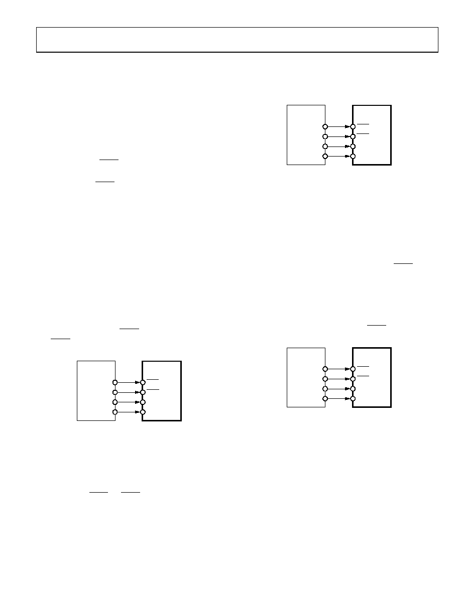
AD5530/AD5531 TO MC68HC11 INTERFACE
Transmission is initiated by writing a word to the Tx register
after the SPORT has been enabled. As the data is clocked out of
the DSP on the rising edge of SCLK, no glue logic is required to
interface the DSP to the DAC. In the interface shown, the DAC
output is updated using the
Figure 25 shows an example of a serial interface between the
AD5530/AD5531 and the MC68HC11 microcontroller. SCK of
the MC68HC11 drives the SCLK of the DAC, and the MOSI
output drives the serial data lines, SDIN. SYNC is driven from
one of the port lines, in this case PC7.
LDAC pin via the DSP. Alternatively,
the LDAC input could be tied permanently low and then the
update takes place automatically when TFS is taken high.
AD5530/
AD55311
MC68HC111
1ADDITIONAL PINS OMITTED FOR CLARITY.
LDAC
PC6
SYNC
PC7
SDIN
MOSI
SCLK
SCK
00
93
8-
0
25
AD5530/
AD55311
ADSP-2101/
ADSP-21031
1ADDITIONAL PINS OMITTED FOR CLARITY.
LDAC
FO
SYNC
TFS
SDIN
DT
SCLK
00
93
8-
0
23
Figure 25. AD5530/AD5531 to MC68HC11 Interface
The MC68HC11 is configured for master mode, MSTR = 1,
CPOL = 0, and CPHA = 1. When data is transferred to the part,
PC7 is taken low and data is transmitted MSB first. Data
appearing on the MOSI output is valid on the falling edge of SCK.
Eight falling clock edges occur in the transmit cycle, so to load the
required 16-bit word, PC7 is not brought high until the second
8-bit word has been transferred to the DAC input shift register.
Figure 23. AD5530/AD5531 to ADSP-21xx Interface
AD5530/AD5531 TO 8051 INTERFACE
A serial interface between the AD5530/AD5531 and the 8051 is
shown in Figure 24. TxD of the 8051 drives SCLK of the
AD5530/AD5531, while RxD drives the serial data line, SDIN.
P3.3 and P3.4 are bit-programmable pins on the serial port and
are used to drive SYNC and LDAC, respectively.
相关PDF资料 |
PDF描述 |
|---|---|
| AD5324BRMZ-REEL7 | IC DAC 12BIT QUAD VOUT 10MSOP TR |
| AD5324BRMZ-REEL | IC DAC 12BIT QUAD VOUT 10MSOP TR |
| AD5318ARU | IC DAC 10BIT OCTAL W/BUF 16TSSOP |
| LTC1655CS8#TRPBF | IC D/A CONV 16BIT R-R 8-SOIC |
| VI-B6N-MV-B1 | CONVERTER MOD DC/DC 18.5V 150W |
相关代理商/技术参数 |
参数描述 |
|---|---|
| AD5531BRUZ-REEL1 | 制造商:AD 制造商全称:Analog Devices 功能描述:Serial Input, Voltage Output 12-/14-Bit Digital-to-Analog Converters |
| AD5531BRUZ-REEL7 | 功能描述:IC DAC 14BIT SRL IN/VOUT 16TSSOP RoHS:是 类别:集成电路 (IC) >> 数据采集 - 数模转换器 系列:- 标准包装:47 系列:- 设置时间:2µs 位数:14 数据接口:并联 转换器数目:1 电压电源:单电源 功率耗散(最大):55µW 工作温度:-40°C ~ 85°C 安装类型:表面贴装 封装/外壳:28-SSOP(0.209",5.30mm 宽) 供应商设备封装:28-SSOP 包装:管件 输出数目和类型:1 电流,单极;1 电流,双极 采样率(每秒):* |
| AD5531BRUZ-REEL71 | 制造商:AD 制造商全称:Analog Devices 功能描述:Serial Input, Voltage Output 12-/14-Bit Digital-to-Analog Converters |
| AD5532 | 制造商:AD 制造商全称:Analog Devices 功能描述:32-Channel, 14-Bit Voltage-Output DAC |
| AD5532-1 | 制造商:AD 制造商全称:Analog Devices 功能描述:32-Channel, 14-Bit Voltage-Output DAC |
发布紧急采购,3分钟左右您将得到回复。