- 您现在的位置:买卖IC网 > PDF目录8610 > AD5542BRZ-REEL7 (Analog Devices Inc)IC DAC 16BIT SERIAL IN 14SOIC PDF资料下载
参数资料
| 型号: | AD5542BRZ-REEL7 |
| 厂商: | Analog Devices Inc |
| 文件页数: | 6/20页 |
| 文件大小: | 0K |
| 描述: | IC DAC 16BIT SERIAL IN 14SOIC |
| 产品培训模块: | Data Converter Fundamentals DAC Architectures |
| 设计资源: | High Precision Digital-to-Analog Conversion Using the 16-Bit AD5542/1, ADR421, and AD8628 (CN0079) How to Achieve High Precision Voltage Level Setting Using AD5541A/42A (CN0169) |
| 标准包装: | 1,000 |
| 设置时间: | 1µs |
| 位数: | 16 |
| 数据接口: | 串行 |
| 转换器数目: | 1 |
| 电压电源: | 单电源 |
| 功率耗散(最大): | 825µW |
| 工作温度: | -40°C ~ 85°C |
| 安装类型: | 表面贴装 |
| 封装/外壳: | 14-SOIC(0.154",3.90mm 宽) |
| 供应商设备封装: | 14-SOICN |
| 包装: | 带卷 (TR) |
| 输出数目和类型: | 1 电压,单极;1 电压,双极 |
| 采样率(每秒): | 1.5M |
AD5541/AD5542
Data Sheet
Rev. F | Page 14 of 20
MICROPROCESSOR INTERFACING
Microprocessor interfacing to the AD5541/AD5542 is via a
serial bus that uses standard protocol that is compatible with
DSP processors and microcontrollers. The communications
channel requires a 3- or 4-wire interface consisting of a clock
signal, a data signal and a synchronization signal. The
AD5541/AD5542 require a 16-bit data-word with data valid on
the rising edge of SCLK. The DAC update can be done
automatically when all the data is clocked in or it can be done
under control of the LDAC (AD5542 only).
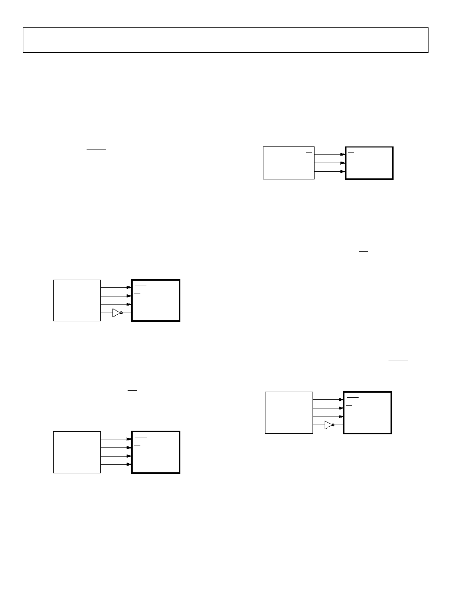
AD5541/AD5542 TO ADSP-21XX INTERFACE
Figure 25 shows a serial interface between the AD5541/AD5542
and the ADSP-21xx. The ADSP-21xx should be set to operate in
the SPORT transmit alternate framing mode. The ADSP-21xx are
programmed through the SPORT control register and should be
configured as follows: internal clock operation, active low
framing, 16-bit word length. Transmission is initiated by
writing a word to the Tx register after the SPORT has been
enabled. As the data is clocked out on each rising edge of the
serial clock, an inverter is required between the DSP and the
DAC, because the AD5541/AD5542 clock data in on the falling
edge of the SCLK.
LDAC**
CS
DIN
SCLK
FO
TFS
DT
SCLK
AD5541/
AD5542*
ADSP-21xx
*ADDITIONAL PINS OMITTED FOR CLARITY.
**AD5542 ONLY.
07557-
025
Figure 25. AD5541/AD5542 to ADSP-21xx Interface
AD5541/AD5542 TO 68HC11/68L11 INTERFACE
Figure 26 shows a serial interface between the AD5541/AD5542
and the 68HC11/68L11 microcontroller. SCK of the 68HC11/
68L11 drives the SCLK of the DAC, and the MOSI output drives
the serial data line serial DIN. The CS signal is driven from one
of the port lines. The 68HC11/68L11 is configured for master
mode: MSTR = 1, CPOL = 0, and CPHA = 0. Data appearing
on the MOSI output is valid on the rising edge of SCK.
LDAC**
CS
DIN
SCLK
PC6
PC7
MOSI
SCK
AD5541/
AD5542*
68HC11/
68L11*
*ADDITIONAL PINS OMITTED FOR CLARITY.
**AD5542 ONLY.
07557-
026
Figure 26. AD5541/AD5542 to 68HC11/68L11 Interface
AD5541/AD5542 TO MICROWIRE INTERFACE
Figure 27 shows an interface between the AD5541/AD5542
and any MICROWIRE-compatible device. Serial data is shifted
out on the falling edge of the serial clock and into the AD5541/
AD5542 on the rising edge of the serial clock. No glue logic is
required because the DAC clocks data into the input shift
register on the rising edge.
DIN
SCLK
SO
SCLK
AD5541/
AD5542*
MICROWIRE*
*ADDITIONAL PINS OMITTED FOR CLARITY.
07557-
027
CS
Figure 27. AD5541/AD5542 to MICROWIRE Interface
AD5541/AD5542 TO 80C51/80L51 INTERFACE
A serial interface between the AD5541/AD5542 and the 80C51/
80L51 microcontroller is shown in Figure 28. TxD of the micro-
controller drives the SCLK of the AD5541/AD5542, and RxD
drives the serial data line of the DAC. P3.3 is a bit programmable
pin on the serial port that is used to drive CS.
The 80C51/80L51 provide the LSB first, whereas the AD5541/
AD5542 expects the MSB of the 16-bit word first. Care should
be taken to ensure the transmit routine takes this into account.
When data is to be transmitted to the DAC, P3.3 is taken low.
Data on RxD is valid on the falling edge of TxD, so the clock
must be inverted as the DAC clocks data into the input shift
register on the rising edge of the serial clock. The 80C51/80L51
transmit data in 8-bit bytes with only eight falling clock edges
occurring in the transmit cycle. As the DAC requires a 16-bit
word, P3.3 must be left low after the first eight bits are transferred,
and brought high after the second byte is transferred. LDAC on
the AD5542 can also be controlled by the 80C51/ 80L51 serial
port output by using another bit programmable pin, P3.4.
LDAC**
CS
DIN
SCLK
P3.4
P3.3
RxD
TxD
AD5541/
AD5542*
80C51/
80L51*
*ADDITIONAL PINS OMITTED FOR CLARITY.
**AD5542 ONLY.
07557-
028
Figure 28. AD5541/AD5542 to 80C51/80L51 Interface
相关PDF资料 |
PDF描述 |
|---|---|
| AD7248AAPZ-REEL | IC DAC 12BIT W/REF 28PLCC |
| LTC2615CGN-1#TRPBF | IC DAC 14BIT R-R OCT 16SSOP |
| AD7545ALPZ-REEL | IC DAC 12BIT W/BUFF MULT 20PLCC |
| AD7548JR-REEL7 | IC DAC 12BIT MONO LC2MOS 20-SOIC |
| LTC2753IUK-14#PBF | IC DAC 14BIT DUAL 48-QFN |
相关代理商/技术参数 |
参数描述 |
|---|---|
| AD5542CR | 功能描述:IC DAC 16BIT SERIAL-IN 14-SOIC RoHS:否 类别:集成电路 (IC) >> 数据采集 - 数模转换器 系列:- 产品培训模块:Data Converter Fundamentals DAC Architectures 标准包装:750 系列:- 设置时间:7µs 位数:16 数据接口:并联 转换器数目:1 电压电源:双 ± 功率耗散(最大):100mW 工作温度:0°C ~ 70°C 安装类型:表面贴装 封装/外壳:28-LCC(J 形引线) 供应商设备封装:28-PLCC(11.51x11.51) 包装:带卷 (TR) 输出数目和类型:1 电压,单极;1 电压,双极 采样率(每秒):143k |
| AD5542CR-REEL7 | 制造商:Rochester Electronics LLC 功能描述:- Tape and Reel |
| AD5542CRZ | 功能描述:IC DAC 16BIT SERIAL-IN 14-SOIC RoHS:是 类别:集成电路 (IC) >> 数据采集 - 数模转换器 系列:- 标准包装:1 系列:- 设置时间:4.5µs 位数:12 数据接口:串行,SPI? 转换器数目:1 电压电源:单电源 功率耗散(最大):- 工作温度:-40°C ~ 125°C 安装类型:表面贴装 封装/外壳:8-SOIC(0.154",3.90mm 宽) 供应商设备封装:8-SOICN 包装:剪切带 (CT) 输出数目和类型:1 电压,单极;1 电压,双极 采样率(每秒):* 其它名称:MCP4921T-E/SNCTMCP4921T-E/SNRCTMCP4921T-E/SNRCT-ND |
| AD5542CRZ-REEL7 | 制造商:AD 制造商全称:Analog Devices 功能描述:2.7 V to 5.5 V, Serial-Input, Voltage-Output, 16-Bit DACs |
| AD5542JR | 功能描述:IC DAC 16BIT SERIAL-IN 14-SOIC RoHS:否 类别:集成电路 (IC) >> 数据采集 - 数模转换器 系列:- 标准包装:2,400 系列:- 设置时间:- 位数:18 数据接口:串行 转换器数目:3 电压电源:模拟和数字 功率耗散(最大):- 工作温度:-40°C ~ 85°C 安装类型:表面贴装 封装/外壳:36-TFBGA 供应商设备封装:36-TFBGA 包装:带卷 (TR) 输出数目和类型:* 采样率(每秒):* |
发布紧急采购,3分钟左右您将得到回复。