参数资料
| 型号: | AD5542CR |
| 厂商: | Analog Devices Inc |
| 文件页数: | 17/20页 |
| 文件大小: | 0K |
| 描述: | IC DAC 16BIT SERIAL-IN 14-SOIC |
| 产品培训模块: | Data Converter Fundamentals DAC Architectures |
| 设计资源: | High Precision Digital-to-Analog Conversion Using the 16-Bit AD5542/1, ADR421, and AD8628 (CN0079) How to Achieve High Precision Voltage Level Setting Using AD5541A/42A (CN0169) |
| 标准包装: | 1 |
| 设置时间: | 1µs |
| 位数: | 16 |
| 数据接口: | 串行 |
| 转换器数目: | 1 |
| 电压电源: | 单电源 |
| 功率耗散(最大): | 825µW |
| 工作温度: | -40°C ~ 85°C |
| 安装类型: | 表面贴装 |
| 封装/外壳: | 14-SOIC(0.154",3.90mm 宽) |
| 供应商设备封装: | 14-SOICN |
| 包装: | 管件 |
| 输出数目和类型: | 1 电压,单极;1 电压,双极 |
| 采样率(每秒): | 1.5M |
AD5541/AD5542
Data Sheet
Rev. F | Page 6 of 20
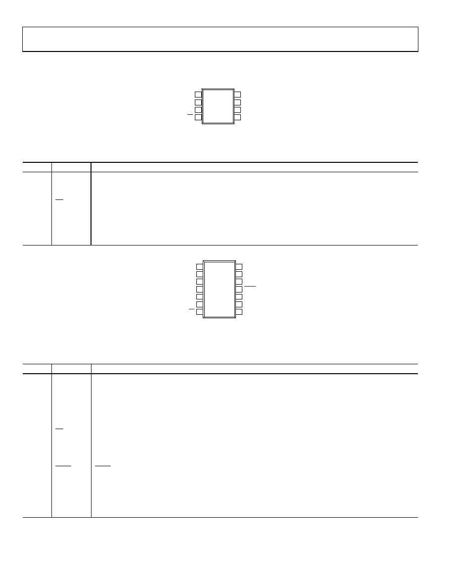
PIN CONFIGURATIONS AND FUNCTION DESCRIPTIONS
VOUT 1
AGND
2
REF
3
CS
4
VDD
8
DGND
7
DIN
6
SCLK
5
AD5541
TOP VIEW
(Not to Scale)
07557-
004
Figure 4. AD5541 Pin Configuration
Table 5. AD5541 Pin Function Descriptions
Pin No.
Mnemonic
Description
1
V
OUT
Analog Output Voltage from the DAC.
2
AGND
Ground Reference Point for Analog Circuitry.
3
REF
Voltage Reference Input for the DAC. Connect to an external 2.5 V reference. Reference can range from 2 V to V
DD.
4
CS
Logic Input Signal. The chip select signal is used to frame the serial data input.
5
SCLK
Clock Input. Data is clocked into the input register on the rising edge of SCLK. Duty cycle must be between 40% and 60%.
6
DIN
Serial Data Input. This device accepts 16-bit words. Data is clocked into the input register on the rising edge of SCLK.
7
DGND
Digital Ground. Ground reference for digital circuitry.
8
V
DD
Analog Supply Voltage, 5 V ± 10%.
07557-
005
RFB
1
VOUT 2
AGNDF
3
AGNDS
4
VDD
14
INV
13
DGND
12
LDAC
11
REFS
5
DIN
10
REFF
6
NC
9
CS
7
SCLK
8
NC = NO CONNECT
AD5542
TOP VIEW
(Not to Scale)
Figure 5. AD5542 Pin Configuration
Table 6. AD5542 Pin Function Descriptions
Pin No.
Mnemonic
Description
1
RFB
Feedback Resistor Pin. In bipolar mode, connect this pin to the external op amp output.
2
V
OUT
Analog Output Voltage from the DAC.
3
AGNDF
Ground Reference Point for Analog Circuitry (Force).
4
AGNDS
Ground Reference Point for Analog Circuitry (Sense).
5
REFS
Voltage Reference Input (Sense) for the DAC. Connect to an external 2.5 V reference. Reference can range from 2 V to V
DD.
6
REFF
Voltage Reference Input (Force) for the DAC. Connect to an external 2.5 V reference. Reference can range from 2 V to V
DD.
7
CS
Logic Input Signal. The chip select signal is used to frame the serial data input.
8
SCLK
Clock Input. Data is clocked into the input register on the rising edge of SCLK. Duty cycle must be between 40% and 60%.
9
NC
No Connect.
10
DIN
Serial Data Input. This device accepts 16-bit words. Data is clocked into the input register on the rising edge of SCLK.
11
LDAC
LDAC Input. When this input is taken low, the DAC register is simultaneously updated with the contents of the
input register.
12
DGND
Digital Ground. Ground reference for digital circuitry.
13
INV
Connected to the Internal Scaling Resistors of the DAC. Connect the INV pin to external op amps inverting input in
bipolar mode.
14
V
DD
Analog Supply Voltage, 5 V ± 10%.
相关PDF资料 |
PDF描述 |
|---|---|
| AD5543BR | IC DAC 16BIT SRLIN/CUR OUT 8SOIC |
| AD5543SRMZ-EP | IC DAC 16BIT SRL 8MSOP |
| AD5544ARS | IC DAC 16BIT QUAD SRL IN 28-SSOP |
| AD5546BRU | IC DAC 16BIT PARALL IN 28-TSSOP |
| AD5551BR | IC DAC 14BIT SERIAL-IN 8-SOIC |
相关代理商/技术参数 |
参数描述 |
|---|---|
| AD5542CR-REEL7 | 制造商:Rochester Electronics LLC 功能描述:- Tape and Reel |
| AD5542CRZ | 功能描述:IC DAC 16BIT SERIAL-IN 14-SOIC RoHS:是 类别:集成电路 (IC) >> 数据采集 - 数模转换器 系列:- 标准包装:1 系列:- 设置时间:4.5µs 位数:12 数据接口:串行,SPI? 转换器数目:1 电压电源:单电源 功率耗散(最大):- 工作温度:-40°C ~ 125°C 安装类型:表面贴装 封装/外壳:8-SOIC(0.154",3.90mm 宽) 供应商设备封装:8-SOICN 包装:剪切带 (CT) 输出数目和类型:1 电压,单极;1 电压,双极 采样率(每秒):* 其它名称:MCP4921T-E/SNCTMCP4921T-E/SNRCTMCP4921T-E/SNRCT-ND |
| AD5542CRZ-REEL7 | 制造商:AD 制造商全称:Analog Devices 功能描述:2.7 V to 5.5 V, Serial-Input, Voltage-Output, 16-Bit DACs |
| AD5542JR | 功能描述:IC DAC 16BIT SERIAL-IN 14-SOIC RoHS:否 类别:集成电路 (IC) >> 数据采集 - 数模转换器 系列:- 标准包装:2,400 系列:- 设置时间:- 位数:18 数据接口:串行 转换器数目:3 电压电源:模拟和数字 功率耗散(最大):- 工作温度:-40°C ~ 85°C 安装类型:表面贴装 封装/外壳:36-TFBGA 供应商设备封装:36-TFBGA 包装:带卷 (TR) 输出数目和类型:* 采样率(每秒):* |
| AD5542JR-REEL7 | 功能描述:IC DAC 16BIT SERIAL-IN 14-SOIC RoHS:否 类别:集成电路 (IC) >> 数据采集 - 数模转换器 系列:- 标准包装:2,400 系列:- 设置时间:- 位数:18 数据接口:串行 转换器数目:3 电压电源:模拟和数字 功率耗散(最大):- 工作温度:-40°C ~ 85°C 安装类型:表面贴装 封装/外壳:36-TFBGA 供应商设备封装:36-TFBGA 包装:带卷 (TR) 输出数目和类型:* 采样率(每秒):* |
发布紧急采购,3分钟左右您将得到回复。