- 您现在的位置:买卖IC网 > PDF目录8629 > AD5542JRZ-REEL7 (Analog Devices Inc)IC DAC 16BIT SERIAL IN 14SOIC PDF资料下载
参数资料
| 型号: | AD5542JRZ-REEL7 |
| 厂商: | Analog Devices Inc |
| 文件页数: | 3/20页 |
| 文件大小: | 0K |
| 描述: | IC DAC 16BIT SERIAL IN 14SOIC |
| 产品培训模块: | Data Converter Fundamentals DAC Architectures |
| 设计资源: | High Precision Digital-to-Analog Conversion Using the 16-Bit AD5542/1, ADR421, and AD8628 (CN0079) How to Achieve High Precision Voltage Level Setting Using AD5541A/42A (CN0169) |
| 标准包装: | 1,000 |
| 设置时间: | 1µs |
| 位数: | 16 |
| 数据接口: | 串行 |
| 转换器数目: | 1 |
| 电压电源: | 单电源 |
| 功率耗散(最大): | 825µW |
| 工作温度: | -40°C ~ 85°C |
| 安装类型: | 表面贴装 |
| 封装/外壳: | 14-SOIC(0.154",3.90mm 宽) |
| 供应商设备封装: | 14-SOICN |
| 包装: | 带卷 (TR) |
| 输出数目和类型: | 1 电压,单极;1 电压,双极 |
| 采样率(每秒): | 1.5M |
Data Sheet
AD5541/AD5542
Rev. F | Page 11 of 20
THEORY OF OPERATION
The AD5541/AD5542 are single, 16-bit, serial input, voltage
output DACs. They operate from a single supply ranging from
2.7 V to 5.5 V and consume typically 125 A with a supply of
5 V. Data is written to these devices in a 16-bit word format,
via a 3- or 4-wire serial interface. To ensure a known power-up
state, these parts are designed with a power-on reset function.
In unipolar mode, the output is reset to 0 V; in bipolar mode,
the AD5542 output is set to VREF. Kelvin sense connections for
the reference and analog ground are included on the AD5542.
DIGITAL-TO-ANALOG SECTION
The DAC architecture consists of two matched DAC sections.
A simplified circuit diagram is shown in Figure 22. The DAC
architecture of the AD5541/AD5542 is segmented. The four
MSBs of the 16-bit data-word are decoded to drive 15 switches,
E1 to E15. Each switch connects one of 15 matched resistors to
either AGND or VREF. The remaining 12 bits of the data-word
drive switches S0 to S11 of a 12-bit voltage mode R-2R ladder
network.
2R . . . . .
S1 . . . . .
2R
S11
2R
E1
2R . . . . .
E2 . . . . .
2R
S0
2R
E15
R
VREF
VOUT
12-BIT R-2R LADDER
FOUR MSBs DECODED
INTO 15 EQUAL SEGMENTS
07557-
022
Figure 22. DAC Architecture
With this type of DAC configuration, the output impedance
is independent of code, while the input impedance seen by
the reference is heavily code dependent. The output voltage is
dependent on the reference voltage, as shown in the following
equation:
N
REF
OUT
D
V
2
×
=
where:
D is the decimal data-word loaded to the DAC register.
N is the resolution of the DAC.
For a reference of 2.5 V, the equation simplifies to the following:
536
,
65
5
.
2
D
VOUT
×
=
This gives a VOUT of 1.25 V with midscale loaded and 2.5 V with
full-scale loaded to the DAC.
The LSB size is VREF/65,536.
SERIAL INTERFACE
The AD5541/AD5542 are controlled by a versatile 3- or 4-wire
serial interface that operates at clock rates up to 25 MHz and is
compatible with SPI, QSPI, MICROWIRE, and DSP interface
standards. The timing diagram is shown in Figure 3. Input data
is framed by the chip select input, CS. After a high-to-low
transition on CS, data is shifted synchronously and latched into
the input register on the rising edge of the serial clock, SCLK.
Data is loaded MSB first in 16-bit words. After 16 data bits have
been loaded into the serial input register, a low-to-high transition
on CS transfers the contents of the shift register to the DAC. Data
can be loaded to the part only while CS is low.
The AD5542 has an LDAC function that allows the DAC latch
to be updated asynchronously by bringing LDAC low after CS
goes high. LDAC should be maintained high while data is written
to the shift register. Alternatively, LDAC can be tied perma-
nently low to update the DAC synchronously. With LDAC tied
permanently low, the rising edge of CS loads the data to the DAC.
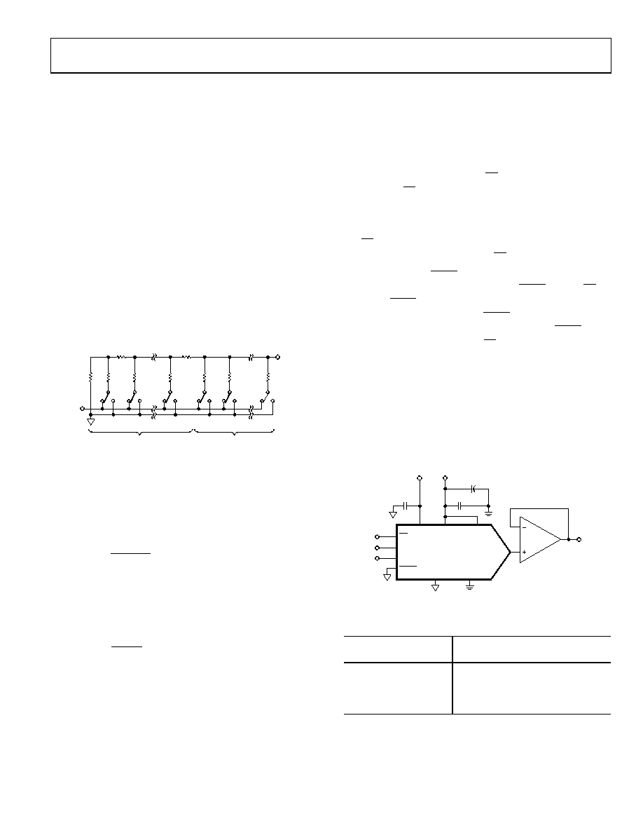
UNIPOLAR OUTPUT OPERATION
These DACs are capable of driving unbuffered loads of 60 k.
Unbuffered operation results in low supply current, typically
300 μA, and a low offset error. The AD5541 provides a unipolar
output swing ranging from 0 V to VREF. The AD5542 can be
configured to output both unipolar and bipolar voltages. Figure 23
shows a typical unipolar output voltage circuit. The code table
for this mode of operation is shown in Table 7.
07557-
023
OUT
REFS*
REF(REFF*)
DGND
AGND
VDD
DIN
SCLK
LDAC*
CS
AD5541/AD5542
AD820/
OP196
+
0.1F
10F
UNIPOLAR
OUTPUT
EXTERNAL
OP AMP
2.5V
5V
SERIAL
INTERFACE
*AD5542 ONLY.
Figure 23. Unipolar Output
Table 7. Unipolar Code Table
DAC Latch Contents
MSB
LSB
Analog Output
1111 1111 1111 1111
V
REF × (65,535/65,536)
1000 0000 0000 0000
V
REF × (32,768/65,536) = VREF
0000 0000 0000 0001
V
REF × (1/65,536)
0000 0000 0000 0000
0 V
相关PDF资料 |
PDF描述 |
|---|---|
| AD5541JRZ-REEL7 | IC DAC 16BIT SRL IN/VOUT 8-SOIC |
| ADA4937-2YCPZ-R7 | IC ADC DRIVER DIFF DUAL 24LFCSP |
| AD5412AREZ | IC DAC 12BIT SER 24TSSOP |
| ADA4938-2ACPZ-R7 | IC ADC DRIVER DIFF DUAL 24LFCSP |
| DAC8043A1ESZ | IC DAC 12BIT MULT SRL INP 8SOIC |
相关代理商/技术参数 |
参数描述 |
|---|---|
| AD5542LR | 功能描述:IC DAC 16BIT SERIAL-IN 14-SOIC RoHS:否 类别:集成电路 (IC) >> 数据采集 - 数模转换器 系列:- 产品培训模块:Data Converter Fundamentals DAC Architectures 标准包装:750 系列:- 设置时间:7µs 位数:16 数据接口:并联 转换器数目:1 电压电源:双 ± 功率耗散(最大):100mW 工作温度:0°C ~ 70°C 安装类型:表面贴装 封装/外壳:28-LCC(J 形引线) 供应商设备封装:28-PLCC(11.51x11.51) 包装:带卷 (TR) 输出数目和类型:1 电压,单极;1 电压,双极 采样率(每秒):143k |
| AD5542LRZ | 功能描述:IC DAC 16BIT SERIAL-IN 14-SOIC RoHS:是 类别:集成电路 (IC) >> 数据采集 - 数模转换器 系列:- 产品培训模块:Lead (SnPb) Finish for COTS Obsolescence Mitigation Program 标准包装:50 系列:- 设置时间:4µs 位数:12 数据接口:串行 转换器数目:2 电压电源:单电源 功率耗散(最大):- 工作温度:-40°C ~ 85°C 安装类型:表面贴装 封装/外壳:8-TSSOP,8-MSOP(0.118",3.00mm 宽) 供应商设备封装:8-uMAX 包装:管件 输出数目和类型:2 电压,单极 采样率(每秒):* 产品目录页面:1398 (CN2011-ZH PDF) |
| AD5542LRZ | 制造商:Analog Devices 功能描述:IC 16-BIT DAC |
| AD5543 | 制造商:AD 制造商全称:Analog Devices 功能描述:电流输出/串行输入、16位/14位DAC |
| AD5543_12 | 制造商:AD 制造商全称:Analog Devices 功能描述:Current Output/Serial Input, 16-/14-Bit DACs |
发布紧急采购,3分钟左右您将得到回复。