参数资料
| 型号: | AD5543BRMZ |
| 厂商: | Analog Devices Inc |
| 文件页数: | 4/20页 |
| 文件大小: | 0K |
| 描述: | IC DAC 16BIT SERIAL-IN 8-MSOP |
| 产品培训模块: | Data Converter Fundamentals DAC Architectures |
| 设计资源: | Versatile High Precision Programmable Current Sources Using DACs, Op Amps, and MOSFET Transistors (CN0151) |
| 标准包装: | 50 |
| 设置时间: | 500ns |
| 位数: | 16 |
| 数据接口: | 串行 |
| 转换器数目: | 1 |
| 电压电源: | 单电源 |
| 功率耗散(最大): | 55µW |
| 工作温度: | -40°C ~ 85°C |
| 安装类型: | 表面贴装 |
| 封装/外壳: | 8-TSSOP,8-MSOP(0.118",3.00mm 宽) |
| 供应商设备封装: | 8-MSOP |
| 包装: | 管件 |
| 输出数目和类型: | 1 电流,单极;1 电流,双极 |
| 产品目录页面: | 783 (CN2011-ZH PDF) |
AD5543/AD5553
Data Sheet
Rev. F | Page 12 of 20
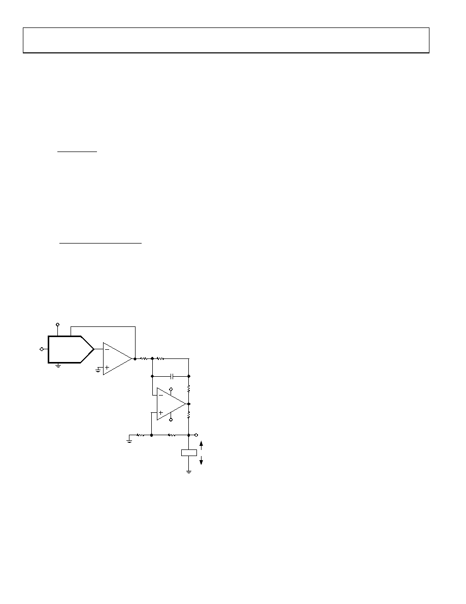
PROGRAMMABLE CURRENT SOURCE
Figure 24 shows a versatile V-I conversion circuit using an
improved Howland current pump. In addition to the precision
current conversion it provides, this circuit enables a bidirectional
current flow and high voltage compliance. This circuit can be used
in 4 mA to 20 mA current transmitters with up to 500 Ω of load. In
Figure 24, it can be shown that if the resistor network is matched,
the load current is
(
)
D
V
R3
R1
R3
R2
I
REF
L
×
+
=
/
(5)
R3 in theory can be made small to achieve the current needed
within the U3 output current driving capability. This circuit is
versatile such that AD8510 can deliver ±20 mA in both directions
and the voltage compliance approaches 15 V, which is limited
mainly by the supply voltages of U3. However, users must pay
attention to the compensation. Without C1, it can be shown
that the output impedance becomes
(
)
(
)
(
)
R3
R2
R1
R3
R2
R1
R2
R1
R3
R1
ZO
+
+
=
'
(6)
If the resistors are perfectly matched, ZO is infinite, which is
desirable, and behaves as an ideal current source. On the other
hand, if they are not matched, ZO can be either positive or negative.
Negative can cause oscillation. As a result, C1 is needed to prevent
the oscillation. For critical applications, C1 could be found
empirically but typically falls in the range of a few picofarads (pF).
U2
U1
AD5543/AD5553
VL
GND
IOUT
RFB
AD8628
AD8510
V+
V–
VREF
LOAD
U3
VDD
VSS
IL
VDD
C1
10pF
R2'
15k
R3'
50
R3
50
R1'
150k
R2
15k
R1
150k
02917-
024
Figure 24. Programmable Current Source with Bidirectional Current Control
and High Voltage Compliance Capabilities
REFERENCE SELECTION
When selecting a reference for use with the AD55xx series of
current output DACs, pay attention to the output voltage,
temperature coefficient specification of the reference. Choosing
a precision reference with a low output temperature coefficient
minimizes error sources. Table 7 lists some of the references
available from Analog Devices, Inc., that are suitable for use
with this range of current output DACs.
AMPLIFIER SELECTION
The primary requirement for the current-steering mode is an
amplifier with low input bias currents and low input offset
voltage. Because of the code-dependent output resistance of the
DAC, the input offset voltage of an op amp is multiplied by the
variable gain of the circuit. A change in this noise gain between
two adjacent digital fractions produces a step change in the
output voltage due to the amplifier’s input offset voltage. This
output voltage change is superimposed upon the desired change
in output between the two codes and gives rise to a differential
linearity error, which, if large enough, can cause the DAC to be
nonmonotonic.
The input bias current of an op amp also generates an offset at
the voltage output because of the bias current flowing in the
feedback resistor, RFB.
Common-mode rejection of the op amp is important in voltage-
switching circuits because it produces a code-dependent error
at the voltage output of the circuit.
Provided that the DAC switches are driven from true wideband
low impedance sources (VIN and AGND), they settle quickly.
Consequently, the slew rate and settling time of a voltage-
switching DAC circuit is determined largely by the output op
amp. To obtain minimum settling time in this configuration,
minimize capacitance at the VREF node (the voltage output node
in this application) of the DAC. This is done by using low input
capacitance buffer amplifiers and careful board design.
Analog Devices offers a wide range of amplifiers for both
precision dc and ac applications, as listed in Table 8 and Table 9.
相关PDF资料 |
PDF描述 |
|---|---|
| VE-B63-MV-F2 | CONVERTER MOD DC/DC 24V 150W |
| VE-JTT-MZ-F1 | CONVERTER MOD DC/DC 6.5V 25W |
| AD5543BRZ | IC DAC 16BIT SRLIN/CUR OUT 8SOIC |
| VE-B63-MV-F1 | CONVERTER MOD DC/DC 24V 150W |
| VE-JT0-MZ-F4 | CONVERTER MOD DC/DC 5V 25W |
相关代理商/技术参数 |
参数描述 |
|---|---|
| AD5543BRMZ | 制造商:Analog Devices 功能描述:DAC, 16BIT, MSOP-8 |
| AD5543BRMZ-REEL7 | 功能描述:IC DAC 16BIT SRLIN/CUR OUT 8MSOP RoHS:是 类别:集成电路 (IC) >> 数据采集 - 数模转换器 系列:- 标准包装:47 系列:- 设置时间:2µs 位数:14 数据接口:并联 转换器数目:1 电压电源:单电源 功率耗散(最大):55µW 工作温度:-40°C ~ 85°C 安装类型:表面贴装 封装/外壳:28-SSOP(0.209",5.30mm 宽) 供应商设备封装:28-SSOP 包装:管件 输出数目和类型:1 电流,单极;1 电流,双极 采样率(每秒):* |
| AD5543BRZ | 功能描述:IC DAC 16BIT SRLIN/CUR OUT 8SOIC RoHS:是 类别:集成电路 (IC) >> 数据采集 - 数模转换器 系列:- 产品培训模块:Lead (SnPb) Finish for COTS Obsolescence Mitigation Program 标准包装:50 系列:- 设置时间:4µs 位数:12 数据接口:串行 转换器数目:2 电压电源:单电源 功率耗散(最大):- 工作温度:-40°C ~ 85°C 安装类型:表面贴装 封装/外壳:8-TSSOP,8-MSOP(0.118",3.00mm 宽) 供应商设备封装:8-uMAX 包装:管件 输出数目和类型:2 电压,单极 采样率(每秒):* 产品目录页面:1398 (CN2011-ZH PDF) |
| AD5543CRMZ | 功能描述:IC DAC 16BIT SER 8MSOP RoHS:是 类别:集成电路 (IC) >> 数据采集 - 数模转换器 系列:- 产品培训模块:Lead (SnPb) Finish for COTS Obsolescence Mitigation Program 标准包装:50 系列:- 设置时间:4µs 位数:12 数据接口:串行 转换器数目:2 电压电源:单电源 功率耗散(最大):- 工作温度:-40°C ~ 85°C 安装类型:表面贴装 封装/外壳:8-TSSOP,8-MSOP(0.118",3.00mm 宽) 供应商设备封装:8-uMAX 包装:管件 输出数目和类型:2 电压,单极 采样率(每秒):* 产品目录页面:1398 (CN2011-ZH PDF) |
| AD5543CRMZ-REEL7 | 功能描述:IC DAC 16BIT SRL 8MSOP RoHS:是 类别:集成电路 (IC) >> 数据采集 - 数模转换器 系列:- 标准包装:47 系列:- 设置时间:2µs 位数:14 数据接口:并联 转换器数目:1 电压电源:单电源 功率耗散(最大):55µW 工作温度:-40°C ~ 85°C 安装类型:表面贴装 封装/外壳:28-SSOP(0.209",5.30mm 宽) 供应商设备封装:28-SSOP 包装:管件 输出数目和类型:1 电流,单极;1 电流,双极 采样率(每秒):* |
发布紧急采购,3分钟左右您将得到回复。