参数资料
| 型号: | AD5543CRMZ |
| 厂商: | Analog Devices Inc |
| 文件页数: | 2/20页 |
| 文件大小: | 0K |
| 描述: | IC DAC 16BIT SER 8MSOP |
| 设计资源: | Versatile High Precision Programmable Current Sources Using DACs, Op Amps, and MOSFET Transistors (CN0151) |
| 标准包装: | 50 |
| 设置时间: | 500ns |
| 位数: | 16 |
| 数据接口: | 串行 |
| 转换器数目: | 1 |
| 电压电源: | 单电源 |
| 功率耗散(最大): | 55µW |
| 工作温度: | -40°C ~ 85°C |
| 安装类型: | 表面贴装 |
| 封装/外壳: | 8-TSSOP,8-MSOP(0.118",3.00mm 宽) |
| 供应商设备封装: | 8-MSOP |
| 包装: | 管件 |
| 输出数目和类型: | 1 电流,单极;1 电流,双极 |
| 产品目录页面: | 783 (CN2011-ZH PDF) |
AD5543/AD5553
Data Sheet
Rev. F | Page 10 of 20
SERIAL DATA INTERFACE
The AD5543/AD5553 use a 3-wire (CS, SDI, CLK) serial data
interface. New serial data is clocked into the serial input register
in a 16-bit data-word format for the AD5543. The MSB is loaded
first. Table 5 defines the 16 data-word bits. Data is placed on the
SDI pin and clocked into the register on the positive clock edge
of CLK, subject to the data setup-and-hold time requirements
that are specified in the interface timing specifications. Only the
last 16 bits clocked into the serial register are interrogated when
the CS pin is strobed to transfer the serial register data to the DAC
register. Because most microcontrollers output serial data in 8-
bit bytes, two data bytes can be written to the AD5543/AD5553.
After loading the serial register, the rising edge of CS transfers
the serial register data to the DAC register; during this strobe,
the CLK should not be toggled. For the AD5553, with 16-bit
clock cycles, the two LSBs are ignored.
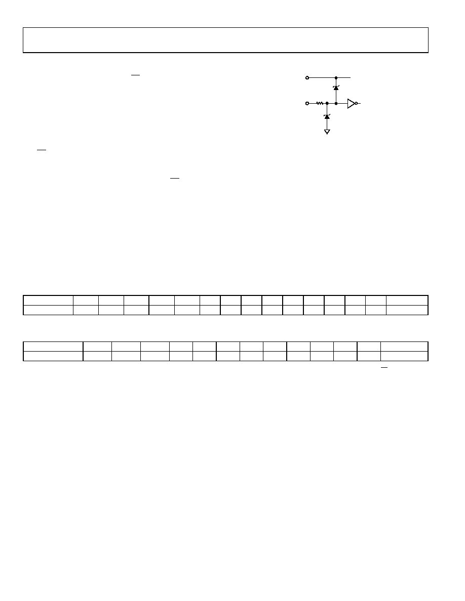
ESD PROTECTION CIRCUITS
All logic input pins contain back-biased ESD protection Zener
diodes that are connected to ground (DGND) and VDD, as
shown in Figure 20.
VDD
DIGITAL
INPUTS
DGND
5k
0
291
7-
0
20
Figure 20. Equivalent ESD Protection Circuits
PCB LAYOUT AND POWER SUPPLY BYPASSING
It is a good practice to employ compact, minimum lead length
PCB layout design. The leads to the input should be as short as
possible to minimize IR drop and stray inductance.
It is also essential to bypass the power supplies with quality
capacitors for optimum stability. Supply leads to the device
should be bypassed with 0.01 μF to 0.1 μF disc or chip ceramic
capacitors. Low ESR 1 μF to 10 μF tantalum or electrolytic
capacitors should also be applied at the supplies to minimize
transient disturbance and filter out low frequency ripple.
The PCB metal traces between VREF and RFB should also be
matched to minimize gain error.
Table 5. AD5543 Serial Input Register Data Format; Data Loaded MSB-First Format
B15 (MSB)
B14
B13
B12
B11
B10
B9
B8
B7
B6
B5
B4
B3
B2
B1
B0 (LSB)
D15
D14
D13
D12
D11
D10
D9
D8
D7
D6
D5
D4
D3
D2
D1
D0
Table 6. AD5553 Serial Input Register Data Format; Data Loaded MSB-First Format
B13 (MSB)1
B12
B11
B10
B9
B8
B7
B6
B5
B4
B3
B2
B1
B0 (LSB)
D13
D12
D11
D10
D9
D8
D7
D6
D5
D4
D3
D2
D1
D0
1 A full 16-bit data-word can be loaded into the AD5553 serial input register, but only the last 14 bits entered are transferred to the DAC register when CS returns to
logic high.
相关PDF资料 |
PDF描述 |
|---|---|
| VE-BNF-MV-F1 | CONVERTER MOD DC/DC 72V 150W |
| VE-BND-MV-F4 | CONVERTER MOD DC/DC 85V 150W |
| M83723/96R1814N | CONN PLUG 14POS STRAIGHT W/PINS |
| VI-J0M-MZ-F4 | CONVERTER MOD DC/DC 10V 25W |
| VE-BND-MV-F1 | CONVERTER MOD DC/DC 85V 150W |
相关代理商/技术参数 |
参数描述 |
|---|---|
| AD5543CRMZ-REEL7 | 功能描述:IC DAC 16BIT SRL 8MSOP RoHS:是 类别:集成电路 (IC) >> 数据采集 - 数模转换器 系列:- 标准包装:47 系列:- 设置时间:2µs 位数:14 数据接口:并联 转换器数目:1 电压电源:单电源 功率耗散(最大):55µW 工作温度:-40°C ~ 85°C 安装类型:表面贴装 封装/外壳:28-SSOP(0.209",5.30mm 宽) 供应商设备封装:28-SSOP 包装:管件 输出数目和类型:1 电流,单极;1 电流,双极 采样率(每秒):* |
| AD5543SRMZ-EP | 功能描述:IC DAC 16BIT SRL 8MSOP RoHS:是 类别:集成电路 (IC) >> 数据采集 - 数模转换器 系列:- 产品培训模块:Lead (SnPb) Finish for COTS Obsolescence Mitigation Program 标准包装:1,000 系列:- 设置时间:1µs 位数:8 数据接口:串行 转换器数目:8 电压电源:双 ± 功率耗散(最大):941mW 工作温度:0°C ~ 70°C 安装类型:表面贴装 封装/外壳:24-SOIC(0.295",7.50mm 宽) 供应商设备封装:24-SOIC W 包装:带卷 (TR) 输出数目和类型:8 电压,单极 采样率(每秒):* |
| AD5544 | 制造商:AD 制造商全称:Analog Devices 功能描述:Quad, Current-Output, Serial-Input 16-/14-Bit DACs |
| AD5544_04 | 制造商:AD 制造商全称:Analog Devices 功能描述:Quad, Current-Output, Serial-Input 16-/14-Bit DACs |
| AD5544_12 | 制造商:AD 制造商全称:Analog Devices 功能描述:Quad, Current-Output, Serial-Input 16-/14-Bit DACs |
发布紧急采购,3分钟左右您将得到回复。