参数资料
| 型号: | AD5547BRU |
| 厂商: | Analog Devices Inc |
| 文件页数: | 19/20页 |
| 文件大小: | 0K |
| 描述: | IC DAC 16BIT DUAL 38-TSSOP |
| 产品培训模块: | Data Converter Fundamentals DAC Architectures |
| 设计资源: | Precision, Unipolar, Inverting Conversion Using AD5547/57 DAC (CN0026) Precision, Unipolar, Noninverting Configuration for the AD5547/57 DAC (CN0027) Precision, Bipolar, Configuration for AD5547/AD5557 DAC (CN0028) |
| 标准包装: | 1 |
| 设置时间: | 500ns |
| 位数: | 16 |
| 数据接口: | 并联 |
| 转换器数目: | 2 |
| 电压电源: | 单电源 |
| 功率耗散(最大): | 55µW |
| 工作温度: | -40°C ~ 125°C |
| 安装类型: | 表面贴装 |
| 封装/外壳: | 38-TFSOP(0.173",4.40mm 宽) |
| 供应商设备封装: | 38-TSSOP |
| 包装: | 管件 |
| 输出数目和类型: | 2 电流,单极;2 电流,双极 |
| 采样率(每秒): | 2M |
AD5547/AD5557
Data Sheet
Rev. D | Page 8 of 20
NC
1
NC
2
ROFSA 3
RFBA 4
R1A 5
VREFA 7
IOUTA 8
AGNDA 9
DGND 10
AGNDB 11
IOUTB 12
VREFB 13
RCOMB 14
R1B 15
RFBB 16
ROFSB 17
18
A0 19
RCOMA 6
WR
NC = NO CONNECT
D0
38
D1
37
D2
36
D3
35
D4
34
D5
33
D6
32
D7
31
D8
30
VDD
29
D9
28
D10
27
D11
26
D12
25
D13
24
23
MSB
22
LDAC
21
A1
20
RS
04452-
004
AD5557
TOP VIEW
(Not to Scale)
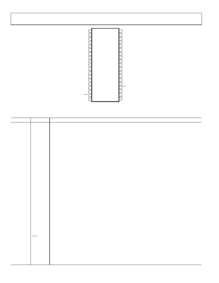
Figure 5. AD5557 Pin Configuration
Table 4. AD5557 Pin Function Descriptions
Pin No.
Mnemonic
Function
1, 2
NC
No Connection. Do not connect anything other than the dummy pads to these pins.
3
R
OFSA
Bipolar Offset Resistor A. Accepts up to ±18 V. In 2-quadrant mode, R
OFSA ties to RFBA. In 4-quadrant mode, ROFSA
ties to R
1A and the external reference.
4
R
FBA
Internal Matching Feedback Resistor A. Connects to the external op amp for I-to-V conversion.
5
R
1A
4-Quandrant Resistor. In 2-quadrant mode, R
1A shorts to the VREFA pin. In 4-quadrant mode, R1A ties to ROFSA. Do
not connect when operating in unipolar mode.
6
R
COMA
Center Tap Point of the Two 4-Quadrant Resistors, R
1A and R2A. In 4-quadrant mode, RCOMA ties to the inverting
node of the reference amplifier. In 2-quadrant mode, R
COMA shorts to the VREFA pin. Do not connect if operating
in unipolar mode.
7
V
REFA
DAC A Reference Input in 2-Quadrant Mode, R2 Terminal in 4-Quadrant Mode. In 2-quadrant mode, V
REFA is the
reference input with constant input resistance vs. code. In 4-quadrant mode, V
REFA is driven by the external
reference amplifier.
8
I
OUTA
DAC A Current Output. Connects to the inverting terminal of external precision I-to-V op amp for voltage
output.
9
AGNDA
DAC A Analog Ground.
10
DGND
Digital Ground.
11
AGNDB
DAC B Analog Ground.
12
I
OUTB
DAC B Current Output. Connects to inverting terminal of external precision I-to-V op amp for voltage output.
13
V
REFB
DAC B Reference Input Pin. Establishes DAC full-scale voltage. Constant input resistance vs. code. If configured
with an external op amp for 4-quadrant multiplying, V
REFB becomes –VREF.
14
R
COMB
Center Tap Point of the Two 4-Quadrant Resistors, R
1B and R2B. In 4-quadrant mode, RCOMB ties to the inverting
node of the reference amplifier. In 2-quadrant mode, R
COMB shorts to the VREFB pin. Do not connect if operating
in unipolar mode.
15
R
1B
4-Quandrant Resistor. In 2-quadrant mode, R
1B shorts to the VREFB pin. In 4-quadrant mode, R1B ties to ROFSB. Do
not connect if operating in unipolar mode.
16
R
FBB
Internal Matching Feedback Resistor B. Connects to external op amp for I-to-V conversion.
17
R
OFSB
Bipolar Offset Resistor B. Accepts up to ±18 V. In 2-quadrant mode, R
OFSB ties to RFBB. In 4-quadrant mode, ROFSB
ties to R
1B and an external reference.
18
WR
Write Control Digital Input In, Active Low. Transfers shift register data to the DAC register on the rising edge.
Signal level must be ≤V
DD + 0.3 V.
19
A0
Address Pin 0. Signal level must be ≤V
DD + 0.3 V.
20
A1
Address Pin 1. Signal level must be ≤V
DD + 0.3 V.
21
LDAC
Digital Input Load DAC Control. Signal level must be ≤V
DD + 0.3 V.
22
MSB
Power-On Reset State. MSB = 0 corresponds to zero-scale reset; MSB = 1 corresponds to midscale reset. The
signal level must be ≤V
DD + 0.3 V.
相关PDF资料 |
PDF描述 |
|---|---|
| AD5560JSVUZ-REEL | IC DPS PROGRAMABLE W/DAC 64TQFP |
| AD557JN | IC DAC 8BIT V-OUT 16-DIP |
| AD561KD | IC DAC 10BIT 5-15V IN MONO 16DIP |
| AD565AKD | IC DAC 12BIT MONO 250NS 24-CDIP |
| AD5663BCPZ-R2 | IC DAC NANO 16BIT DUAL 10-LFCSP |
相关代理商/技术参数 |
参数描述 |
|---|---|
| AD5547BRU-REEL7 | 制造商:Rochester Electronics LLC 功能描述:- Tape and Reel |
| AD5547BRUZ | 功能描述:IC DAC 16BIT DUAL 38-TSSOP RoHS:是 类别:集成电路 (IC) >> 数据采集 - 数模转换器 系列:- 产品培训模块:Lead (SnPb) Finish for COTS Obsolescence Mitigation Program 标准包装:50 系列:- 设置时间:4µs 位数:12 数据接口:串行 转换器数目:2 电压电源:单电源 功率耗散(最大):- 工作温度:-40°C ~ 85°C 安装类型:表面贴装 封装/外壳:8-TSSOP,8-MSOP(0.118",3.00mm 宽) 供应商设备封装:8-uMAX 包装:管件 输出数目和类型:2 电压,单极 采样率(每秒):* 产品目录页面:1398 (CN2011-ZH PDF) |
| AD5547CRUZ | 功能描述:IC DAC 16BIT PAR DUAL 38TSSOP RoHS:是 类别:集成电路 (IC) >> 数据采集 - 数模转换器 系列:- 产品培训模块:Lead (SnPb) Finish for COTS Obsolescence Mitigation Program 标准包装:50 系列:- 设置时间:4µs 位数:12 数据接口:串行 转换器数目:2 电压电源:单电源 功率耗散(最大):- 工作温度:-40°C ~ 85°C 安装类型:表面贴装 封装/外壳:8-TSSOP,8-MSOP(0.118",3.00mm 宽) 供应商设备封装:8-uMAX 包装:管件 输出数目和类型:2 电压,单极 采样率(每秒):* 产品目录页面:1398 (CN2011-ZH PDF) |
| AD5547CRUZ-REEL7 | 功能描述:IC DAC 16BIT PAR DUAL 38TSSOP RoHS:是 类别:集成电路 (IC) >> 数据采集 - 数模转换器 系列:- 产品培训模块:Data Converter Fundamentals DAC Architectures 标准包装:750 系列:- 设置时间:7µs 位数:16 数据接口:并联 转换器数目:1 电压电源:双 ± 功率耗散(最大):100mW 工作温度:0°C ~ 70°C 安装类型:表面贴装 封装/外壳:28-LCC(J 形引线) 供应商设备封装:28-PLCC(11.51x11.51) 包装:带卷 (TR) 输出数目和类型:1 电压,单极;1 电压,双极 采样率(每秒):143k |
| AD5547-EP | 制造商:AD 制造商全称:Analog Devices 功能描述:Dual-Current Output, Parallel Input |
发布紧急采购,3分钟左右您将得到回复。