- 您现在的位置:买卖IC网 > PDF目录8652 > AD5556CRU-REEL7 (Analog Devices Inc)IC DAC 14BIT PARAL IN 28TSSOP TR PDF资料下载
参数资料
| 型号: | AD5556CRU-REEL7 |
| 厂商: | Analog Devices Inc |
| 文件页数: | 3/20页 |
| 文件大小: | 0K |
| 描述: | IC DAC 14BIT PARAL IN 28TSSOP TR |
| 产品培训模块: | Data Converter Fundamentals DAC Architectures |
| 设计资源: | Precision, Unipolar, Inverting Conversion Using AD5546/56 DAC (CN0022) Precision, Bipolar Configuration for the AD5546/56 DAC (CN0024) Precision, Unipolar, Noninverting Configuration for the AD5546/56 DAC (CN0023) Precision, AC Reference Signal Attenuator Using AD5546/56 Multiplying DAC (CN0025) |
| 标准包装: | 1,000 |
| 设置时间: | 500ns |
| 位数: | 14 |
| 数据接口: | 并联 |
| 转换器数目: | 1 |
| 电压电源: | 单电源 |
| 功率耗散(最大): | 55µW |
| 工作温度: | -40°C ~ 125°C |
| 安装类型: | 表面贴装 |
| 封装/外壳: | 28-TSSOP(0.173",4.40mm 宽) |
| 供应商设备封装: | 28-TSSOP |
| 包装: | 带卷 (TR) |
| 输出数目和类型: | 1 电流,单极;1 电流,双极 |
| 采样率(每秒): | 2M |
Data Sheet
AD5546/AD5556
Rev. D | Page 11 of 20
DIGITAL SECTION
The AD5546/AD5556 have 16-/14-bit parallel inputs. The devices are double buffered with 16-/14-bit registers. The double-buffered
feature allows the update of several AD5546/AD5556 simultaneously. For the AD5546, the input register is loaded directly from a 16-bit
controller bus when the WR pin is brought low. The DAC register is updated with data from the input register when LDAC is brought
high. Updating the DAC register updates the DAC output with the new data (see Figure 17). To make both registers transparent, tie WR
low and LDAC high. The asynchronous RS pin resets the part to zero scale if the MSB pin = 0 and to midscale if the MSB pin = 1.
Table 5. AD5546 Parallel Input Data Format
MSB
LSB
Bit Position
B15
B14
B13
B12
B11
B10
B9
B8
B7
B6
B5
B4
B3
B2
B1
B0
Data Word
D15
D14
D13
D12
D11
D10
D9
D8
D7
D6
D5
D4
D3
D2
D1
D0
Table 6. AD5556 Parallel Input Data Format
MSB
LSB
Bit Position
B13
B12
B11
B10
B9
B8
B7
B6
B5
B4
B3
B2
B1
B0
Data Word
D13
D12
D11
D10
D9
D8
D7
D6
D5
D4
D3
D2
D1
D0
Table 7. Control Inputs
RS
WR
LDAC
Register Operation
0
Reset output to 0, with MSB pin = 0 and to midscale with MSB pin = 1.
1
0
Load input register with data bits.
1
Load DAC register with the contents of the input register.
1
0
1
Input and DAC registers are transparent.
1
When LDAC and WR are tied together and programmed as a pulse, the data bits are loaded into the input register on
the falling edge of the pulse and then loaded into the DAC register on the rising edge of the pulse.
1
0
No register operation.
1
X = don’t care.
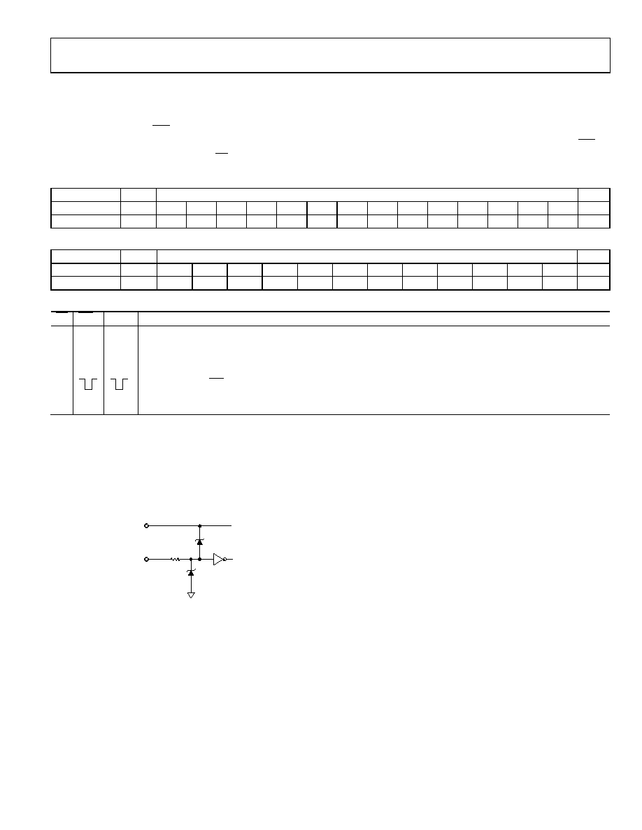
ESD PROTECTION CIRCUITS
All logic input pins contain back-biased ESD protection Zeners
a result, the voltage level of the logic input should not be greater
than the supply voltage.
03810-
020
5k
DIGITAL
INPUTS
DGND
VDD
Figure 18. Equivalent ESD Protection Circuits
AMPLIFIER SELECTION
In addition to offset voltage, the bias current is important in op
amp selection for precision current output DACs. An input bias
current of 30 nA in the op amp contributes to 1 LSB in the
AD5546’s full-scale error. The OP1177 and AD8628 op amps
are good candidates for the I-V conversion.
REFERENCE SELECTION
The initial accuracy and the rated output of the voltage refer-
ence determine the full span adjustment. The initial accuracy is
usually a secondary concern in precision because it can be
trimmed. Figure 23 shows an example of a trimming circuit.
The zero scale error can also be minimized by standard op amp
nulling techniques.
The voltage reference temperature coefficient (TC) and long-
term drift are primary considerations. For example, a 5 V ref-
erence with a TC of 5 ppm/oC means that the output changes by
25 V per degree Celsius. As a result, the reference that operates
at 55oC contributes an additional 750 V full-scale error.
Similarly, the same 5 V reference with a ±50 ppm long-term
drift means that the output may change by ±250 V over time.
Therefore, it is practical to calibrate a system periodically to
maintain its optimum precision.
相关PDF资料 |
PDF描述 |
|---|---|
| IDT74FCT807BTQ | IC CLK BUFFER 1:10 100MHZ 20QSOP |
| VI-J63-MZ-B1 | CONVERTER MOD DC/DC 24V 25W |
| VI-J62-MZ-B1 | CONVERTER MOD DC/DC 15V 25W |
| IDT74FCT807BTPYI8 | IC CLK BUFFER 1:10 100MHZ 20SSOP |
| IDT74FCT807BTPYI | IC CLK BUFFER 1:10 100MHZ 20SSOP |
相关代理商/技术参数 |
参数描述 |
|---|---|
| AD5556CRUZ | 功能描述:IC DAC 14BIT PARALL IN 28-TSSOP RoHS:是 类别:集成电路 (IC) >> 数据采集 - 数模转换器 系列:- 产品培训模块:Lead (SnPb) Finish for COTS Obsolescence Mitigation Program 标准包装:50 系列:- 设置时间:4µs 位数:12 数据接口:串行 转换器数目:2 电压电源:单电源 功率耗散(最大):- 工作温度:-40°C ~ 85°C 安装类型:表面贴装 封装/外壳:8-TSSOP,8-MSOP(0.118",3.00mm 宽) 供应商设备封装:8-uMAX 包装:管件 输出数目和类型:2 电压,单极 采样率(每秒):* 产品目录页面:1398 (CN2011-ZH PDF) |
| AD5556CRUZ | 制造商:Analog Devices 功能描述:IC, DAC, 14BIT, TSSOP-28 |
| AD5557 | 制造商:AD 制造商全称:Analog Devices 功能描述:Dual Current Output, Parallel Input, 16-/14-Bit Multiplying DACs with 4-Quadrant Resistors |
| AD5557CRU | 功能描述:IC DAC 14BIT 2CH I OUT 38TSSOP RoHS:否 类别:集成电路 (IC) >> 数据采集 - 数模转换器 系列:- 产品培训模块:Data Converter Fundamentals DAC Architectures 标准包装:750 系列:- 设置时间:7µs 位数:16 数据接口:并联 转换器数目:1 电压电源:双 ± 功率耗散(最大):100mW 工作温度:0°C ~ 70°C 安装类型:表面贴装 封装/外壳:28-LCC(J 形引线) 供应商设备封装:28-PLCC(11.51x11.51) 包装:带卷 (TR) 输出数目和类型:1 电压,单极;1 电压,双极 采样率(每秒):143k |
| AD5557CRU-REEL7 | 功能描述:IC DAC 14BIT 2CH I OUT 38TSSOP RoHS:否 类别:集成电路 (IC) >> 数据采集 - 数模转换器 系列:- 产品培训模块:Data Converter Fundamentals DAC Architectures 标准包装:750 系列:- 设置时间:7µs 位数:16 数据接口:并联 转换器数目:1 电压电源:双 ± 功率耗散(最大):100mW 工作温度:0°C ~ 70°C 安装类型:表面贴装 封装/外壳:28-LCC(J 形引线) 供应商设备封装:28-PLCC(11.51x11.51) 包装:带卷 (TR) 输出数目和类型:1 电压,单极;1 电压,双极 采样率(每秒):143k |
发布紧急采购,3分钟左右您将得到回复。