参数资料
| 型号: | AD5556CRUZ |
| 厂商: | Analog Devices Inc |
| 文件页数: | 17/20页 |
| 文件大小: | 0K |
| 描述: | IC DAC 14BIT PARALL IN 28-TSSOP |
| 产品培训模块: | Data Converter Fundamentals DAC Architectures |
| 设计资源: | Precision, Unipolar, Inverting Conversion Using AD5546/56 DAC (CN0022) Precision, Bipolar Configuration for the AD5546/56 DAC (CN0024) Precision, Unipolar, Noninverting Configuration for the AD5546/56 DAC (CN0023) Precision, AC Reference Signal Attenuator Using AD5546/56 Multiplying DAC (CN0025) |
| 标准包装: | 50 |
| 设置时间: | 500ns |
| 位数: | 14 |
| 数据接口: | 并联 |
| 转换器数目: | 1 |
| 电压电源: | 单电源 |
| 功率耗散(最大): | 55µW |
| 工作温度: | -40°C ~ 125°C |
| 安装类型: | 表面贴装 |
| 封装/外壳: | 28-TSSOP(0.173",4.40mm 宽) |
| 供应商设备封装: | 28-TSSOP |
| 包装: | 管件 |
| 输出数目和类型: | 1 电流,单极;1 电流,双极 |
| 采样率(每秒): | 2M |
| 产品目录页面: | 783 (CN2011-ZH PDF) |
AD5546/AD5556
Data Sheet
Rev. D | Page 6 of 20
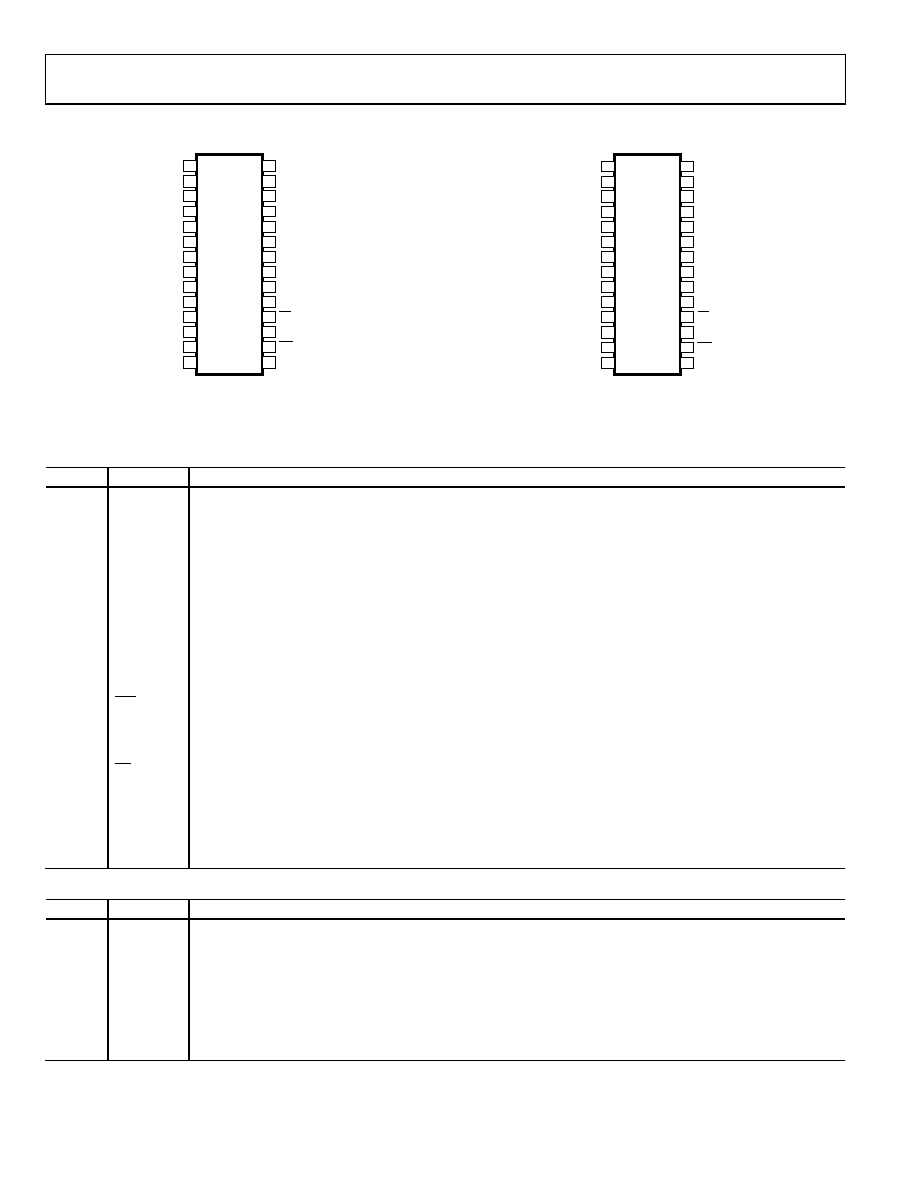
PIN CONFIGURATIONS AND FUNCTION DESCRIPTIONS
03810-
003
AD5546
TOP VIEW
(Not to Scale)
D7
1
VDD
28
D6
2
D8
27
D5
3
D9
26
D4
4
D10
25
D3
5
D11
24
D2
6
D12
23
D1
7
D13
22
D0
8
D14
21
ROFS 9
D15
20
RFB 10
GND
19
R1 11
RS
18
RCOM 12
MSB
17
REF 13
WR
16
IOUT 14
LDAC
15
Figure 4. AD5546 Pin Configuration
03810-
004
AD5556
TOP VIEW
(Not to Scale)
NC = NO CONNECT
D5
1
VDD
28
D4
2
D6
27
D3
3
D7
26
D2
4
D8
25
D1
5
D9
24
D0
6
D10
23
NC
7
D11
22
NC
8
D12
21
ROFS 9
D13
20
RFB 10
GND
19
R1 11
RS
18
RCOM 12
MSB
17
REF 13
WR
16
IOUT 14
LDAC
15
Figure 5. AD5556 Pin Configuration
Table 3. AD5546 Pin Function Descriptions
Pin No.
Mnemonic
Description
1 to 8
D7 to D0
Digital Input Data Bits[D7: D0]. The signal level must be ≤ VDD + 0.3 V.
9
ROFS
Bipolar Offset Resistor. Accepts up to ±18 V. In two-quadrant mode, ties to RFB. In four-quadrant mode, ties to R1
and the external reference.
10
RFB
Internal Matching Feedback Resistor. Connects to the output of an external op amp for I-V conversion.
11
R1
Four-Quadrant Resistor R1. In two-quadrant mode, shorts to the REF pin. In four-quadrant mode, ties to ROFS.
12
RCOM
Center Tap Point of Two Four-Quadrant Resistors, R1 and R2. In four-quadrant mode, ties to the inverting node of
the reference amplifier. In two-quadrant mode, shorts to the REF pin.
13
REF
DAC Reference Input in Two-Quadrant Mode and R2 Terminal in Four-Quadrant Mode. In two-quadrant mode, this
pin is the reference input with constant input resistance vs. code. In four-quadrant mode, this pin is driven by the
external reference amplifier.
14
IOUT
DAC Current Output. Connects to the inverting node of an external op amp for I-V conversion.
15
LDAC
Digital Input Load DAC Control. Signal level must be ≤ VDD + 0.3 V.
16
WR
Write Control Digital Input in Active Low. Transfers shift-register data to the DAC register on the rising edge. The
signal level must be ≤ VDD + 0.3 V.
17
MSB
Power-On Reset State. MSB = 0 resets at zero scale; MSB = 1 resets at midscale. The signal level must be
≤ VDD + 0.3 V.
18
RS
Reset in Active Low. Resets to zero scale if MSB = 0, and resets to midscale if MSB = 1. The signal level must be
≤ VDD + 0.3 V.
19
GND
Analog and Digital Grounds.
20 to 21
D15 to D14
Digital Input Data Bits[D15:D14]. The signal level must be ≤ VDD + 0.3 V.
22 to 27
D13 to D8
Digital Input Data Bits[D13:D8]. The signal level must be ≤ VDD + 0.3 V.
28
VDD
Positive Power Supply Input. Specified range of operation: 2.7 V to 5.5 V.
Table 4. AD5556 Pin Function Descriptions
Pin No.
Mnemonic
Description
1 to 6
D5 to D0
Digital Input Data Bits[D5:D0]. The signal level must be
≤ VDD+0.3 V.
7 to 8
NC
No Connection. The user should not connect anything other than dummy pads on these terminals.
9
ROFS
Bipolar Offset Resistor. Accepts up to ±18 V. In two-quadrant mode, ties to RFB. In four-quadrant mode, ties to R1
and the external reference.
10
RFB
Internal Matching Feedback Resistor. Connects to the output of an external op amp for I-V conversion.
11
R1
Four-Quadrant Resistor R1. In two-quadrant mode, shorts to the REF pin. In four-quadrant mode, ties to ROFS.
12
RCOM
Center Tap Point of Two Four-Quadrant Resistors, R1 and R2. In four-quadrant mode, ties to the inverting node of
the reference amplifier. In two-quadrant mode, shorts to the REF pin.
相关PDF资料 |
PDF描述 |
|---|---|
| VI-B0W-MY-F1 | CONVERTER MOD DC/DC 5.5V 50W |
| ADV7125KSTZ140 | IC DAC VIDEO 3-CH 140MHZ 48LQFP |
| VE-26N-MW-F2 | CONVERTER MOD DC/DC 18.5V 100W |
| AD5420AREZ | IC DAC 16BIT 1CH SER 24TSSOP |
| VI-B0V-MY-F4 | CONVERTER MOD DC/DC 5.8V 50W |
相关代理商/技术参数 |
参数描述 |
|---|---|
| AD5556CRUZ | 制造商:Analog Devices 功能描述:IC, DAC, 14BIT, TSSOP-28 |
| AD5557 | 制造商:AD 制造商全称:Analog Devices 功能描述:Dual Current Output, Parallel Input, 16-/14-Bit Multiplying DACs with 4-Quadrant Resistors |
| AD5557CRU | 功能描述:IC DAC 14BIT 2CH I OUT 38TSSOP RoHS:否 类别:集成电路 (IC) >> 数据采集 - 数模转换器 系列:- 产品培训模块:Data Converter Fundamentals DAC Architectures 标准包装:750 系列:- 设置时间:7µs 位数:16 数据接口:并联 转换器数目:1 电压电源:双 ± 功率耗散(最大):100mW 工作温度:0°C ~ 70°C 安装类型:表面贴装 封装/外壳:28-LCC(J 形引线) 供应商设备封装:28-PLCC(11.51x11.51) 包装:带卷 (TR) 输出数目和类型:1 电压,单极;1 电压,双极 采样率(每秒):143k |
| AD5557CRU-REEL7 | 功能描述:IC DAC 14BIT 2CH I OUT 38TSSOP RoHS:否 类别:集成电路 (IC) >> 数据采集 - 数模转换器 系列:- 产品培训模块:Data Converter Fundamentals DAC Architectures 标准包装:750 系列:- 设置时间:7µs 位数:16 数据接口:并联 转换器数目:1 电压电源:双 ± 功率耗散(最大):100mW 工作温度:0°C ~ 70°C 安装类型:表面贴装 封装/外壳:28-LCC(J 形引线) 供应商设备封装:28-PLCC(11.51x11.51) 包装:带卷 (TR) 输出数目和类型:1 电压,单极;1 电压,双极 采样率(每秒):143k |
| AD5557CRUZ | 功能描述:IC DAC 14BIT 2CH I OUT 38TSSOP RoHS:是 类别:集成电路 (IC) >> 数据采集 - 数模转换器 系列:- 标准包装:1 系列:- 设置时间:4.5µs 位数:12 数据接口:串行,SPI? 转换器数目:1 电压电源:单电源 功率耗散(最大):- 工作温度:-40°C ~ 125°C 安装类型:表面贴装 封装/外壳:8-SOIC(0.154",3.90mm 宽) 供应商设备封装:8-SOICN 包装:剪切带 (CT) 输出数目和类型:1 电压,单极;1 电压,双极 采样率(每秒):* 其它名称:MCP4921T-E/SNCTMCP4921T-E/SNRCTMCP4921T-E/SNRCT-ND |
发布紧急采购,3分钟左右您将得到回复。