- 您现在的位置:买卖IC网 > PDF目录8584 > AD5570ARS-REEL (Analog Devices Inc)IC DAC 16BIT SRL IN/VOUT 16-SSOP PDF资料下载
参数资料
| 型号: | AD5570ARS-REEL |
| 厂商: | Analog Devices Inc |
| 文件页数: | 1/24页 |
| 文件大小: | 0K |
| 描述: | IC DAC 16BIT SRL IN/VOUT 16-SSOP |
| 产品培训模块: | Data Converter Fundamentals DAC Architectures |
| 标准包装: | 1,500 |
| 设置时间: | 12µs |
| 位数: | 16 |
| 数据接口: | 串行 |
| 转换器数目: | 1 |
| 电压电源: | 双 ± |
| 功率耗散(最大): | 150mW |
| 工作温度: | -40°C ~ 85°C |
| 安装类型: | 表面贴装 |
| 封装/外壳: | 16-SSOP(0.209",5.30mm 宽) |
| 供应商设备封装: | 16-SSOP |
| 包装: | 带卷 (TR) |
| 输出数目和类型: | 1 电压,双极 |
| 采样率(每秒): | 83k |
True Accuracy, 16-Bit ±12 V/±15 V,
Serial Input Voltage Output DAC
AD5570
Rev. C
Information furnished by Analog Devices is believed to be accurate and reliable. However, no
responsibilityis assumedbyAnalogDevicesforitsuse,norforanyinfringements of patents or other
rightsofthirdpartiesthatmayresultfromitsuse.Specificationssubjecttochangewithoutnotice.No
license is granted by implication or otherwise under any patent or patent rights of Analog Devices.
Trademarksandregisteredtrademarksarethepropertyoftheirrespectiveowners.
One Technology Way, P.O. Box 9106, Norwood, MA 02062-9106, U.S.A.
Tel: 781.329.4700
www.analog.com
Fax: 781.461.3113
2010 Analog Devices, Inc. All rights reserved.
FEATURES
Full 16-bit performance
1 LSB maximum INL and DNL
Output voltage range up to ±14 V
On-board reference buffers, eliminating the need for a
negative reference
Controlled output during power-on
Temperature ranges of 40°C to +85°C for A/B version/40°C
to +125°C for W/Y version
Settling time of 10 μs to 0.003%
Clear function to 0 V
Asynchronous update of outputs (LDAC pin)
Power-on reset
Serial data output for daisy chaining
Data readback facility
5 kV HBM ESD classification
APPLICATIONS
Industrial automation
Automatic test equipment
Process control
Data acquisition systems
General-purpose instrumentation
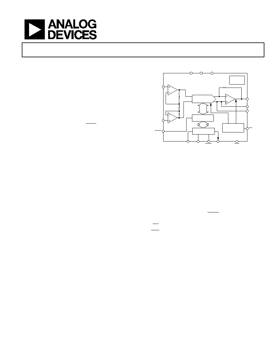
FUNCTIONAL BLOCK DIAGRAM
VOUT
VDD
DGND
AD5570
REFIN
REFGND
LDAC
SDIN
CLR
SCLK
SYNC
PD
DAC REGISTER
SHIFT REGISTER
POWER-DOWN
CONTROL LOGIC
POWER-ON
RESET
SDO
VSS
2R
AGND
AGNDS
R
16-BIT
DAC
0
37
60
-0
01
Figure 1.
GENERAL DESCRIPTION
The AD5570 is a single 16-bit serial input, voltage output DAC
that operates from supply voltages of ±11.4 V up to ±16.5 V.
Integral linearity (INL) and differential nonlinearity (DNL) are
accurate to 1 LSB. During power-up, when the supply voltages
are changing, VOUT is clamped to 0 V via a low impedance path.
The AD5570 DAC comes complete with a set of reference
buffers. The reference buffers allow a single, positive reference
to be used. The voltage on REFIN is gained up and inverted
internally to give the positive and negative reference for the
DAC core. Having the reference buffers on-chip eliminates the
need for external components such as inverters, precision
amplifiers, and resistors, thereby reducing the overall solution
size and cost.
The AD5570 uses a versatile 3-wire interface that is compatible
with SPI, QSPI, MICROWIRE, and DSP interface standards.
Data is presented to the part as a 16-bit serial word. Serial data
is available on the SDO pin for daisy-chaining purposes. Data
readback allows the user to read the contents of the DAC
register via the SDO pin.
Features on the AD5570 include LDAC which is used to update
the output of the DAC. The device also has a power-down pin
(PD), allowing the DAC to be put into a low power state, and a
CLR pin that allows the output to be cleared to 0 V.
The AD5570 is available in a 16-lead SSOP.
PRODUCT HIGHLIGHTS
1.
1 LSB maximum INL and DNL.
2.
Buffered voltage output up to ±14 V.
3.
Output controlled during power-up.
4.
On-board reference buffers.
5.
Wide temperature range of 40°C to +125°C.
6.
5 kV HBM ESD classification.
相关PDF资料 |
PDF描述 |
|---|---|
| AD8146ACPZ-R2 | IC DRIVER TRPL DIFF VID 24LFCSP |
| AD7543JN | IC DAC 12BIT SRL INP MULT 16-DIP |
| VE-B4Y-MY-B1 | CONVERTER MOD DC/DC 3.3V 33W |
| AD8582AR | IC DAC 12BIT DUAL 5V 24-SOIC |
| VE-B4Y-MX-B1 | CONVERTER MOD DC/DC 3.3V 49.5W |
相关代理商/技术参数 |
参数描述 |
|---|---|
| AD5570ARS-REEL7 | 功能描述:IC DAC 16BIT SRL IN/VOUT 16-SSOP RoHS:否 类别:集成电路 (IC) >> 数据采集 - 数模转换器 系列:- 标准包装:2,400 系列:- 设置时间:- 位数:18 数据接口:串行 转换器数目:3 电压电源:模拟和数字 功率耗散(最大):- 工作温度:-40°C ~ 85°C 安装类型:表面贴装 封装/外壳:36-TFBGA 供应商设备封装:36-TFBGA 包装:带卷 (TR) 输出数目和类型:* 采样率(每秒):* |
| AD5570ARSZ | 功能描述:IC DAC 16BIT SERIAL IN 16SSOP RoHS:是 类别:集成电路 (IC) >> 数据采集 - 数模转换器 系列:- 标准包装:1 系列:- 设置时间:4.5µs 位数:12 数据接口:串行,SPI? 转换器数目:1 电压电源:单电源 功率耗散(最大):- 工作温度:-40°C ~ 125°C 安装类型:表面贴装 封装/外壳:8-SOIC(0.154",3.90mm 宽) 供应商设备封装:8-SOICN 包装:剪切带 (CT) 输出数目和类型:1 电压,单极;1 电压,双极 采样率(每秒):* 其它名称:MCP4921T-E/SNCTMCP4921T-E/SNRCTMCP4921T-E/SNRCT-ND |
| AD5570ARSZ-REEL | 功能描述:IC DAC 16BIT SERIAL IN 16SSOP RoHS:是 类别:集成电路 (IC) >> 数据采集 - 数模转换器 系列:- 产品培训模块:Data Converter Fundamentals DAC Architectures 标准包装:750 系列:- 设置时间:7µs 位数:16 数据接口:并联 转换器数目:1 电压电源:双 ± 功率耗散(最大):100mW 工作温度:0°C ~ 70°C 安装类型:表面贴装 封装/外壳:28-LCC(J 形引线) 供应商设备封装:28-PLCC(11.51x11.51) 包装:带卷 (TR) 输出数目和类型:1 电压,单极;1 电压,双极 采样率(每秒):143k |
| AD5570ARSZ-REEL7 | 功能描述:IC DAC 16BIT SERIAL IN 16SSOP RoHS:是 类别:集成电路 (IC) >> 数据采集 - 数模转换器 系列:- 产品培训模块:Data Converter Fundamentals DAC Architectures 标准包装:750 系列:- 设置时间:7µs 位数:16 数据接口:并联 转换器数目:1 电压电源:双 ± 功率耗散(最大):100mW 工作温度:0°C ~ 70°C 安装类型:表面贴装 封装/外壳:28-LCC(J 形引线) 供应商设备封装:28-PLCC(11.51x11.51) 包装:带卷 (TR) 输出数目和类型:1 电压,单极;1 电压,双极 采样率(每秒):143k |
| AD5570BRS | 功能描述:IC DAC 16BIT SERIAL IN 16SSOP RoHS:否 类别:集成电路 (IC) >> 数据采集 - 数模转换器 系列:- 产品培训模块:Lead (SnPb) Finish for COTS Obsolescence Mitigation Program 标准包装:1,000 系列:- 设置时间:1µs 位数:8 数据接口:串行 转换器数目:8 电压电源:双 ± 功率耗散(最大):941mW 工作温度:0°C ~ 70°C 安装类型:表面贴装 封装/外壳:24-SOIC(0.295",7.50mm 宽) 供应商设备封装:24-SOIC W 包装:带卷 (TR) 输出数目和类型:8 电压,单极 采样率(每秒):* |
发布紧急采购,3分钟左右您将得到回复。