- 您现在的位置:买卖IC网 > PDF目录10803 > AD557JP-REEL (Analog Devices Inc)IC DAC 8BIT 5V OUT AMP 20-PLCC PDF资料下载
参数资料
| 型号: | AD557JP-REEL |
| 厂商: | Analog Devices Inc |
| 文件页数: | 4/6页 |
| 文件大小: | 0K |
| 描述: | IC DAC 8BIT 5V OUT AMP 20-PLCC |
| 产品培训模块: | Data Converter Fundamentals DAC Architectures |
| 产品变化通告: | Product Discontinuance 27/Oct/2011 |
| 标准包装: | 1,000 |
| 系列: | DACPORT® |
| 设置时间: | 800ns |
| 位数: | 8 |
| 数据接口: | 并联 |
| 转换器数目: | 1 |
| 电压电源: | 单电源 |
| 功率耗散(最大): | 125mW |
| 工作温度: | 0°C ~ 70°C |
| 安装类型: | 表面贴装 |
| 封装/外壳: | 20-LCC(J 形引线) |
| 供应商设备封装: | 20-PLCC(9x9) |
| 包装: | 带卷 (TR) |
| 输出数目和类型: | 1 电压,单极;1 电压,双极 |
| 采样率(每秒): | 1.25M |
AD557
REV. B
–4–
Timing and Control
The AD557 has data input latches that simplify interface to 8-
and 16-bit data buses. These latches are controlled by Chip
Enable (
CE) and Chip Select (CS) inputs. CE and CS are inter-
nally “NORed” so that the latches transmit input data to the
DAC section when both
CE and CS are at Logic “0.” If the
application does not involve a data bus, a “00” condition allows
for direct operation of the DAC. When either
CE or CS go to
Logic “1,” the input data is latched into the registers and held
until both
CE and CS return to “0.” (Unused CE or CS inputs
should be tied to ground.) The truth table is given in Table I.
The logic function is also shown in Figure 6.
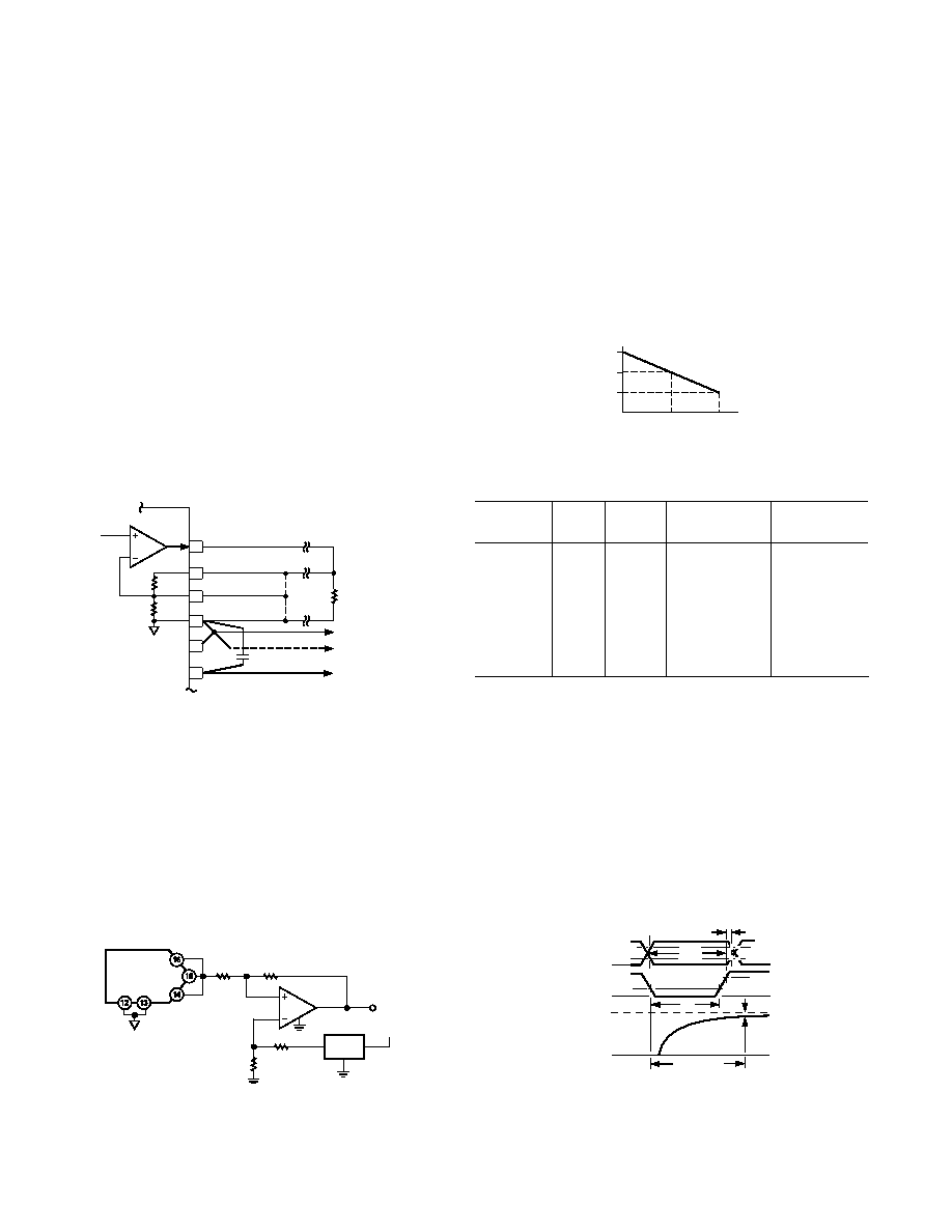
VOUT
7.5
5.0
2.5
00H
80H
FFH
AD557 INPUT CODE
Figure 6. AD557 Input Code vs. Level Shifted Output in a
“False” Ground Configuration
Table I. AD557 Control Logic Truth Table
Latch
Input Data
CE
CS
DAC Data
Condition
0
“Transparent”
1
0
1
“Transparent”
0
g
0
Latching
1
g
0
1
Latching
00
g
0
Latching
10
g
1
Latching
X
1
X
Previous Data
Latched
X
1
Previous Data
Latched
NOTES
X = Does not matter
g = Logic Threshold at Positive-Going Transition
In a level-triggered latch such as that used in the AD557, there
is an interaction between the data setup and hold times and
the width of the enable pulse. In an effort to reduce the time
required to test all possible combinations in production, the
AD557 is tested with tDS = tW = 225 ns at 25
°C and 300 ns at
TMIN and TMAX, with tDH = 10 ns at all temperatures. Failure to
comply with these specifications may result in data not being
latched properly.
Figure 7 shows the timing for the data and control signals,
CE
and
CS are identical in timing as well as in function.
DATA
INPUTS
CS OR CE
DAC
V OUTPUT
0.8V
2.0V
1/2 LSB
tW
tSETTLING
tDH
tW = STROBE PULSEWIDTH = 225ns min
tDH = DATA HOLD TIME = 10ns min
tDS = DATA SETUP TIME = 225ns min
tSETTLING = DAC SETTLING TIME TO
1/2 LSB
tDS
Figure 7. AD557 Timing
APPLICATIONS
Grounding and Bypassing
All precision converter products require careful application of
good grounding practices to maintain full rated performance.
Because the AD557 is intended for application in microcom-
puter systems where digital noise is prevalent, special care must
be taken to assure that its inherent precision is realized.
The AD557 has two ground (common) pins; this minimizes
ground drops and noise in the analog signal path. Figure 4
shows how the ground connections should be made.
It is often advisable to maintain separate analog and digital
grounds throughout a complete system, tying them common in
one place only. If the common tie-point is remote and acciden-
tal disconnection of that one common tie-point occurs due to
card removal with power on, a large differential voltage between
the two commons could develop. To protect devices that inter-
face to both digital and analog parts of the system, such as the
AD557, it is recommended that common ground tie-points
should be provided at each such device. If only one system
ground can be connected directly to the AD557, it is recom-
mended that analog common be selected.
16
15
14
13
OUTPUT
AMP
VOUT
VOUT SENSE A
VOUT SENSE B
GND
12
11
GND
+VCC
0.1 F
TO SYSTEM GND
(SEE TEXT)
TO SYSTEM VCC
RL
Figure 4. Recommended Grounding and Bypassing
Using a “False” Ground
Many applications, such as disk drives, require servo control
voltages that swing on either side of a “false” ground. This
ground is usually created by dividing the 12 V supply equally
and calling the midpoint voltage “ground.”
Figure 5 shows an easy and inexpensive way to implement this.
The AD586 is used to provide a stable 5 V reference from the
system’s 12 V supply. The op amp shown likewise operates from
a single (12 V) supply available in the system. The resulting out-
put at the VOUT node is
±2.5 V around the “false” ground point
of 5 V. AD557 input code vs. VOUT is shown in Figure 6.
AD557
100k
200k
1/4 LM324
VOUT
AD586
VIN
2
12V
5V
“FALSE”
GROUND
6
4
Figure 5. Level Shifting the AD557 Output Around a
“False” Ground
相关PDF资料 |
PDF描述 |
|---|---|
| LTC2855IGN#PBF | IC TXRX RS485/RS422 16-SSOP |
| LTC2855IDE#PBF | IC TXRX RS485/RS422 12-DFN |
| LTC2861IGN#PBF | IC TXRX RS485 20MBPS 16-SSOP |
| KSZ8001L | IC TXRX PHY 10/100 3.3V 48-LQFP |
| KSZ8001SL | TXRX 10/100 LINKMD 3.3V 48-SSOP |
相关代理商/技术参数 |
参数描述 |
|---|---|
| AD557JP-REEL7 | 功能描述:IC DAC 8BIT 5V OUT AMP 20-PLCC RoHS:否 类别:集成电路 (IC) >> 数据采集 - 数模转换器 系列:DACPORT® 标准包装:2,400 系列:- 设置时间:- 位数:18 数据接口:串行 转换器数目:3 电压电源:模拟和数字 功率耗散(最大):- 工作温度:-40°C ~ 85°C 安装类型:表面贴装 封装/外壳:36-TFBGA 供应商设备封装:36-TFBGA 包装:带卷 (TR) 输出数目和类型:* 采样率(每秒):* |
| AD557JPZ | 功能描述:IC DAC 8BIT V-OUT 20-PLCC RoHS:是 类别:集成电路 (IC) >> 数据采集 - 数模转换器 系列:DACPORT® 产品培训模块:Lead (SnPb) Finish for COTS Obsolescence Mitigation Program 标准包装:50 系列:- 设置时间:4µs 位数:12 数据接口:串行 转换器数目:2 电压电源:单电源 功率耗散(最大):- 工作温度:-40°C ~ 85°C 安装类型:表面贴装 封装/外壳:8-TSSOP,8-MSOP(0.118",3.00mm 宽) 供应商设备封装:8-uMAX 包装:管件 输出数目和类型:2 电压,单极 采样率(每秒):* 产品目录页面:1398 (CN2011-ZH PDF) |
| AD557JPZ-REEL | 功能描述:IC DAC 8BIT 5V OUT AMP 20-PLCC RoHS:是 类别:集成电路 (IC) >> 数据采集 - 数模转换器 系列:DACPORT® 产品培训模块:LTC263x 12-, 10-, and 8-Bit VOUT DAC Family 特色产品:LTC2636 - Octal 12-/10-/8-Bit SPI VOUT DACs with 10ppm/°C Reference 标准包装:91 系列:- 设置时间:4µs 位数:10 数据接口:MICROWIRE?,串行,SPI? 转换器数目:8 电压电源:单电源 功率耗散(最大):2.7mW 工作温度:-40°C ~ 85°C 安装类型:表面贴装 封装/外壳:14-WFDFN 裸露焊盘 供应商设备封装:14-DFN-EP(4x3) 包装:管件 输出数目和类型:8 电压,单极 采样率(每秒):* |
| AD557JPZ-REEL7 | 功能描述:IC DAC 8BIT 5V OUT AMP 20-PLCC RoHS:是 类别:集成电路 (IC) >> 数据采集 - 数模转换器 系列:DACPORT® 标准包装:47 系列:- 设置时间:2µs 位数:14 数据接口:并联 转换器数目:1 电压电源:单电源 功率耗散(最大):55µW 工作温度:-40°C ~ 85°C 安装类型:表面贴装 封装/外壳:28-SSOP(0.209",5.30mm 宽) 供应商设备封装:28-SSOP 包装:管件 输出数目和类型:1 电流,单极;1 电流,双极 采样率(每秒):* |
| AD558 | 制造商:AD 制造商全称:Analog Devices 功能描述:DACPORT Low Cost, Complete uP-Compatible 8-Bit DAC |
发布紧急采购,3分钟左右您将得到回复。