- 您现在的位置:买卖IC网 > PDF目录8657 > AD557JPZ-REEL7 (Analog Devices Inc)IC DAC 8BIT 5V OUT AMP 20-PLCC PDF资料下载
参数资料
| 型号: | AD557JPZ-REEL7 |
| 厂商: | Analog Devices Inc |
| 文件页数: | 3/6页 |
| 文件大小: | 0K |
| 描述: | IC DAC 8BIT 5V OUT AMP 20-PLCC |
| 产品培训模块: | Data Converter Fundamentals DAC Architectures |
| 标准包装: | 250 |
| 系列: | DACPORT® |
| 设置时间: | 800ns |
| 位数: | 8 |
| 数据接口: | 并联 |
| 转换器数目: | 1 |
| 电压电源: | 单电源 |
| 功率耗散(最大): | 125mW |
| 工作温度: | 0°C ~ 70°C |
| 安装类型: | 表面贴装 |
| 封装/外壳: | 20-LCC(J 形引线) |
| 供应商设备封装: | 20-PLCC(9x9) |
| 包装: | 带卷 (TR) |
| 输出数目和类型: | 1 电压,单极;1 电压,双极 |
| 采样率(每秒): | 1.25M |
AD557
REV. B
–3–
CONNECTING THE AD557
The AD557 has been configured for low cost and ease of appli-
cation. All reference, output amplifier and logic connections are
made internally. In addition, all calibration trims are performed
at the factory assuring specified accuracy without user trims.
The only connection decision to be made by the user is whether
the output range desired is unipolar or bipolar. Clean circuit
board layout is facilitated by isolating all digital bit inputs on
one side of the package; analog outputs are on the opposite side.
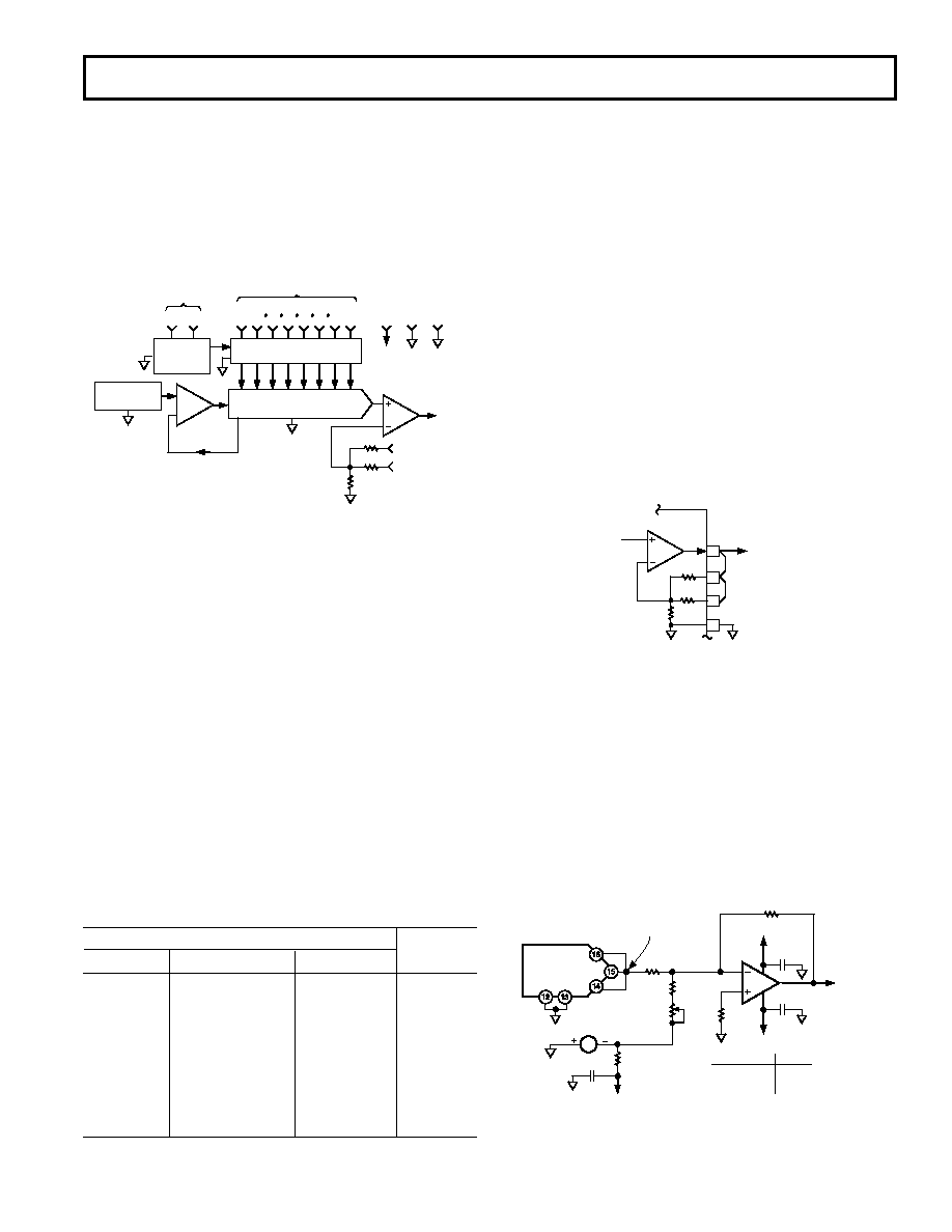
UNIPOLAR 0 V TO 2.56 V OUTPUT RANGE
Figure 2 shows the configuration for the 0 V to 2.56 V full-
scale output range. Because of its precise factory calibration, the
AD557 is intended to be operated without user trims for gain
and offset; therefore, no provisions have been made for such user
trims. If a small increase in scale is required, however, it may be
accomplished by slightly altering the effective gain of the output
buffer. A resistor in series with VOUT SENSE will increase the
output range. Note that decreasing the scale by putting a resistor
in series with GND will not work properly due to the code-
dependent currents in GND. Adjusting offset by injecting dc at
GND is not recommended for the same reason.
16
15
14
13
OUTPUT
AMP
VOUT
VOUT SENSE A
VOUT SENSE B
GND
Figure 2. 0 V to 2.56 V Output Range
BIPOLAR –1.28 V TO +1.28 V OUTPUT RANGE
The AD557 was designed for operation from a single power
supply and is thus capable of providing only a unipolar 0 V to
2.56 V output range. If a negative supply is available, bipolar
output ranges may be achieved by suitable output offsetting and
scaling. Figure 3 shows how a
± 1.28 V output range may be
achieved when a –5 V power supply is available. The offset is
provided by the AD589 precision 1.2 V reference which will
operate from a 5 V supply. The AD711 output amplifier can
provide the necessary
±1.28 V output swing from ±5 V supplies.
Coding is complementary offset binary.
–1.2V
4.7k
0.01 F
AD589
–5V
VIN
AD557
VOUT = 0V TO 2.56V
5k
4.53k
1.5k
500
BIPOLAR
OFFSET
ADJUST
0.01 F
AD711
–5V
+5V
VO
+1.28 TO
–1.27
INPUT CODE
00000000
10000000
11111111
VOUT
+1.28V
0V
–1.27V
Figure 3. Bipolar Operation of AD557 from
±5 V Supplies
CIRCUIT DESCRIPTION
The AD557 consists of four major functional blocks fabricated
on a single monolithic chip (see Figure 1). The main D/A con-
verter section uses eight equally weighted laser-trimmed current
sources switched into a silicon-chromium thin-film R/2R resistor
ladder network to give a direct but unbuffered 0 mV to 400 mV
output range. The transistors that form the DAC switches are
PNPs; this allows direct positive-voltage logic interface and a
zero-based output range.
BIT1
(MSB)
BIT8
(LSB)
GND
CS CE
CONTROL
INPUTS
DIGITAL INPUT DATA (BUS)
+V
CC
l2L
CONTROL
LOGIC
8-BIT VOLTAGE-SWITCHING
D-TO-A CONVERTER
OUTPUT
AMP
CONTROL
AMP
BAND-GAP
REFERENCE
VOUT
VOUT SENSE A
VOUT SENSE B
l2L LATCHES
GND
Figure 1. Functional Block Diagram
The high-speed output buffer amplifier is operated in the nonin-
verting mode with gain determined by the user-connections
at the output range select pin. The gain-setting application
resistors are thin film laser trimmed to match and track the
DAC resistors and to assure precise initial calibration of the out-
put range, 0 V to 2.56 V. The amplifier output stage is an
NPN transistor with passive pull-down for zero-based output
capability with a single power supply.
The internal precision voltage reference is of the patented
band-gap type. This design produces a reference voltage of
1.2 V and thus, unlike 6.3 V temperature-compensated Zeners,
may be operated from a single, low-voltage logic power supply.
The microprocessor interface logic consists of an 8-bit data
latch and control circuitry. Low power, small geometry and high
speed are advantages of the I
2L design as applied to this section.
I
2L is bipolar process compatible so that the performance of the
analog sections need not be compromised to provide on-chip
logic capabilities. The control logic allows the latches to be
operated from a decoded microprocessor address and write sig-
nal. If the application does not involve a
P or data bus, wiring
CS and CE to ground renders the latches “transparent” for
direct DAC access.
Digital Input Code
Output
Binary
Hexadecimal
Decimal
Voltage
0000 0000
00
0
0000 0001
01
1
0.010 V
0000 0010
02
2
0.020 V
0000 1111
0F
15
0.150 V
0001 0000
10
16
0.160 V
0111 1111
7F
127
1.270 V
1000 0000
80
128
1.280 V
1100 0000
C0
192
1.920 V
1111 1111
FF
255
2.55 V
相关PDF资料 |
PDF描述 |
|---|---|
| LTC1446IS8#TRPBF | IC D/A CONV 12BIT R-R DUAL 8SOIC |
| LTC1446IS8#TR | IC DAC 12BIT DUAL R-R MPWR 8SOIC |
| AD7545AKRZ-REEL | IC DAC 12BIT W/BUFF MULT 20SOIC |
| IDT49FCT3805PY8 | IC CLK BUFFER 1:5 100MHZ 20-SSOP |
| AD5422AREZ-REEL | IC DAC 16BIT SRL 24TSSOP |
相关代理商/技术参数 |
参数描述 |
|---|---|
| AD558 | 制造商:AD 制造商全称:Analog Devices 功能描述:DACPORT Low Cost, Complete uP-Compatible 8-Bit DAC |
| AD5582 | 制造商:AD 制造商全称:Analog Devices 功能描述:QUAD, Parallel-Input, Voltage Output, 12-/10-Bit Digital-to-Analog Converter |
| AD5582YRU-REEL7 | 制造商:AD 制造商全称:Analog Devices 功能描述:QUAD, Parallel-Input, Voltage Output, 12-/10-Bit Digital-to-Analog Converter |
| AD5582YRV | 制造商:Analog Devices 功能描述:QUAD 12BIT DAC SMD 5582 TSSOP48 |
发布紧急采购,3分钟左右您将得到回复。