- 您现在的位置:买卖IC网 > PDF目录10786 > AD5582YRVZ-REEL (Analog Devices Inc)IC DAC 12BIT PARALLEL IN 48TSSOP PDF资料下载
参数资料
| 型号: | AD5582YRVZ-REEL |
| 厂商: | Analog Devices Inc |
| 文件页数: | 8/20页 |
| 文件大小: | 0K |
| 描述: | IC DAC 12BIT PARALLEL IN 48TSSOP |
| 产品培训模块: | Data Converter Fundamentals DAC Architectures |
| 产品变化通告: | Product Discontinuance 27/Oct/2011 |
| 标准包装: | 2,500 |
| 设置时间: | 5µs |
| 位数: | 12 |
| 数据接口: | 并联 |
| 转换器数目: | 4 |
| 电压电源: | 模拟和数字,双 ± |
| 功率耗散(最大): | 30mW |
| 工作温度: | -40°C ~ 125°C |
| 安装类型: | 表面贴装 |
| 封装/外壳: | 48-TFSOP(0.240",6.10mm 宽) |
| 供应商设备封装: | 48-TSSOP |
| 包装: | 带卷 (TR) |
| 输出数目和类型: | 4 电压,单极;4 电压,双极 |
| 采样率(每秒): | 200k |
REV. A
–16–
AD5582/AD5583
Reset
The
RS function can be used either at power-up or at any time
during operation. The
RS function has priority over any other
digital inputs. This pin is active low and sets the DAC output
registers to either zero scale or midscale, determined by the state
of the MSB. The reset to midscale is useful when the DAC is
configured for bipolar references and the output will be reset to 0 V.
Output Amplifiers
Unlike many voltage output DACs, the AD5582/AD5583 feature
buffered voltage outputs with high output current driving capa-
bility. Each output is capable of both sourcing and sinking
±20 mA,
eliminating the need for external buffers when driving any capaci-
tive loads without oscillation. These amplifiers also have short
circuit protection.
Glitch
The worst-case glitch of the AD5582 occurs at the transitions
between midscale (1000 0000 0000B) to midscale minus 1
(0111 1111 1111B), or vice versa. The glitch energy is mea-
sured as 100 mV
1
ms or equivalent to 100 nV-s. Such glitch
occurs in a shorter duration than the settling time and therefore
most applications will be immune to such an effect without a
deglitcher.
Layout and Power Supply Bypassing
It is a good practice to employ compact, minimum lead length
PCB layout design. The leads to the input should be as short as
possible to minimize IR drop and stray inductance.
It is also essential to bypass the power supplies with quality capaci-
tors for optimum stability. Supply leads to the device should be
bypassed with 0.01
mF to 0.1 mF disc or chip ceramics capacitors.
Low ESR 1
mF to 10 mF tantalum or electrolytic capacitors should
also be applied at the supplies to minimize transient disturbance.
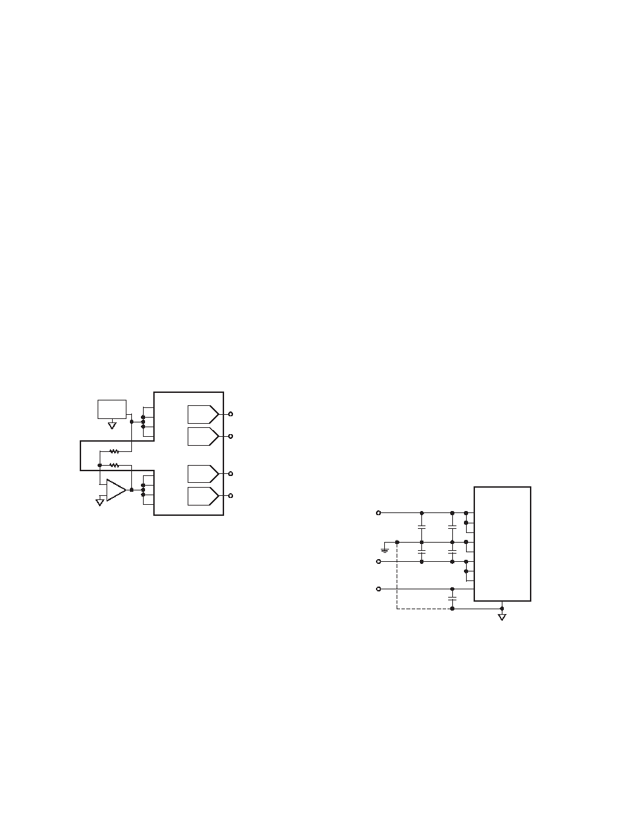
The AD5582/AD5583 optimize internal layout design to reduce
die area so that all analog supply pins are required to be con-
nected externally. See Figure 5.
VDD1
VDD2
VDD3
AGND1
AGND2
VSS1
VSS2
VSS3
AD5582/
AD5583
C2
0.1 F
C4
0.1 F
C1
10 F
C3
10 F
+
C5
0.1 F
DGND
VDD
VSS
DVDD
Figure 5. Power Supply Configurations
APPLICATIONS
Programmable Current Source
AD5582/AD5583 high current capability allow them to be used
directly in programmable current source applications, such as
4 m to 20 mA current transmitter and other general purpose
applications. For higher compliance voltage that is higher than
15 V, Figure 6 shows a versatile V-I conversion circuit using an
improved Howland Current Pump. In addition to the precision
current conversion it provides, this circuit enables a bidirec-
tional current flow and high voltage compliance. The voltage
Since these DACs can be operated at high voltages, the digital
signal levels are therefore controlled separately by the provision
of DVDD. DVDD can be set as low as 2.7 V but no greater than
6.5 V. This allows the DAC to be operable from low level digital
signals generated from a wide range of microcontrollers, FPGA,
and signal processors.
Reference Input
All four channels of DACs allow independent and differential
reference voltages. The flexibility of independent references
allows users to apply a unique reference voltage to each channel.
Similarly, bipolar references can be applied across the differential
references. To maintain optimum accuracy, the difference between
VREFH and VREFL should be greater than 1 V. See TPC 11.
The voltages applied to these reference inputs set the output
voltage limits of all four channels of the DACs, and VREFH must
always be higher than VREFL. VREFH can be set at any voltage from
VREFL + 0.5 V to VDD, while VREFL can be set at any voltage from
VSS to VREFH – 0.5 V. In addition, a symmetrical negative reference
can be generated easily by an external op amp in an inverting
mode with a pair of built-in precision resistors, R1 and R2. These
resistors are matched within
±0.025% for the AD5582 and 0.1%
for the AD5583, which is equivalent to less than 1 LSB mis-
match. Figure 4 shows a simple configuration.
Common reference or references can be applied to all four chan-
nels, but each reference pin should be decoupled with a 0.1
mF
ceramic capacitor mounted close to the pin.
ADR421
REF
DAC A
2.5V
DAC B
2.5V
DAC C
2.5V
DAC D
2.5V
AD5582
VREFHA
VREFHB
VREFHC
VREFHD
VREFLA
VREFLB
VREFLC
VREFLD
+2.5V
R1
R2
–
+
–2.5V
RCT
Figure 4. Using On-Board Matching Resistors
to Generate a Negative Voltage REF
Digital I/O
Digital I/O consists of a 12-/10-bit bidirectional data bus, two
register select inputs, A0 and A1, an R/
W input, a Reset (RS), a
Chip Select (
CS), and a Load DAC (LDAC) input. Control of
the DACs and the bus direction is determined by these inputs
as shown in Table I. All digital pins are TTL/CMOS compat-
ible and all internal registers are level triggered.
The register selects inputs A0 and A1. Decoding of the registers
is enabled by the
CS input. When CS is high, no decoding is
taking place and neither the writing nor the reading of the input
registers is enabled. The loading of the second bank of registers
is controlled by the asynchronous
LDAC input. By taking LDAC
low while
CS is enabled, the individual channel is updated as
single buffer mode, Figure 2a. If
CS is enabled sequentially to
load data into all input registers, then a subsequent
LDAC pulse
will allow all channels to be updated simultaneously as double
buffer mode, Figure 2b.
R/
W controls the writing to and reading from the input register.
相关PDF资料 |
PDF描述 |
|---|---|
| VI-BNV-MX-F1 | CONVERTER MOD DC/DC 5.8V 75W |
| AD5316BRUZ-REEL | IC DAC 10BIT QUAD W/BUFF 16TSSOP |
| VI-JTV-MY-S | CONVERTER MOD DC/DC 5.8V 50W |
| VI-BNV-MW | CONVERTER MOD DC/DC 5.8V 100W |
| VI-21W-IW-S | CONVERTER MOD DC/DC 5.5V 100W |
相关代理商/技术参数 |
参数描述 |
|---|---|
| AD5583 | 制造商:AD 制造商全称:Analog Devices 功能描述:QUAD, Parallel-Input, Voltage Output, 12-/10-Bit Digital-to-Analog Converter |
| AD5583YRU-REEL7 | 制造商:AD 制造商全称:Analog Devices 功能描述:QUAD, Parallel-Input, Voltage Output, 12-/10-Bit Digital-to-Analog Converter |
| AD5583YRV | 制造商:Analog Devices 功能描述:DAC 4-CH R-2R 10-bit 48-Pin TSSOP 制造商:Rochester Electronics LLC 功能描述:QUAD 10BIT DAC PARALLEL IN - Bulk |
| AD5583YRV-REEL | 制造商:Analog Devices 功能描述:DAC 4-CH R-2R 10-bit 48-Pin TSSOP T/R 制造商:Analog Devices 功能描述:DAC 4-CH R-2R 10-BIT 48TSSOP - Tape and Reel 制造商:Rochester Electronics LLC 功能描述:QUAD 10BIT DAC PARALLEL IN - Tape and Reel |
| AD5583YRVZ | 功能描述:IC DAC 10BIT QUAD VOUT 48-TSSOP RoHS:是 类别:集成电路 (IC) >> 数据采集 - 数模转换器 系列:- 产品培训模块:Data Converter Fundamentals DAC Architectures 标准包装:750 系列:- 设置时间:7µs 位数:16 数据接口:并联 转换器数目:1 电压电源:双 ± 功率耗散(最大):100mW 工作温度:0°C ~ 70°C 安装类型:表面贴装 封装/外壳:28-LCC(J 形引线) 供应商设备封装:28-PLCC(11.51x11.51) 包装:带卷 (TR) 输出数目和类型:1 电压,单极;1 电压,双极 采样率(每秒):143k |
发布紧急采购,3分钟左右您将得到回复。