参数资料
| 型号: | AD558JNZ |
| 厂商: | Analog Devices Inc |
| 文件页数: | 4/8页 |
| 文件大小: | 0K |
| 描述: | IC DAC 8BIT V-OUT 16-DIP |
| 产品培训模块: | Data Converter Fundamentals DAC Architectures |
| 标准包装: | 25 |
| 系列: | DACPORT® |
| 设置时间: | 800ns |
| 位数: | 8 |
| 数据接口: | 并联 |
| 转换器数目: | 1 |
| 电压电源: | 单电源 |
| 功率耗散(最大): | 375mW |
| 工作温度: | 0°C ~ 70°C |
| 安装类型: | 通孔 |
| 封装/外壳: | 16-DIP(0.300",7.62mm) |
| 供应商设备封装: | 16-PDIP |
| 包装: | 管件 |
| 输出数目和类型: | 1 电压,单极;1 电压,双极 |
| 采样率(每秒): | * |
| 产品目录页面: | 781 (CN2011-ZH PDF) |
AD558
REV. A
–4–
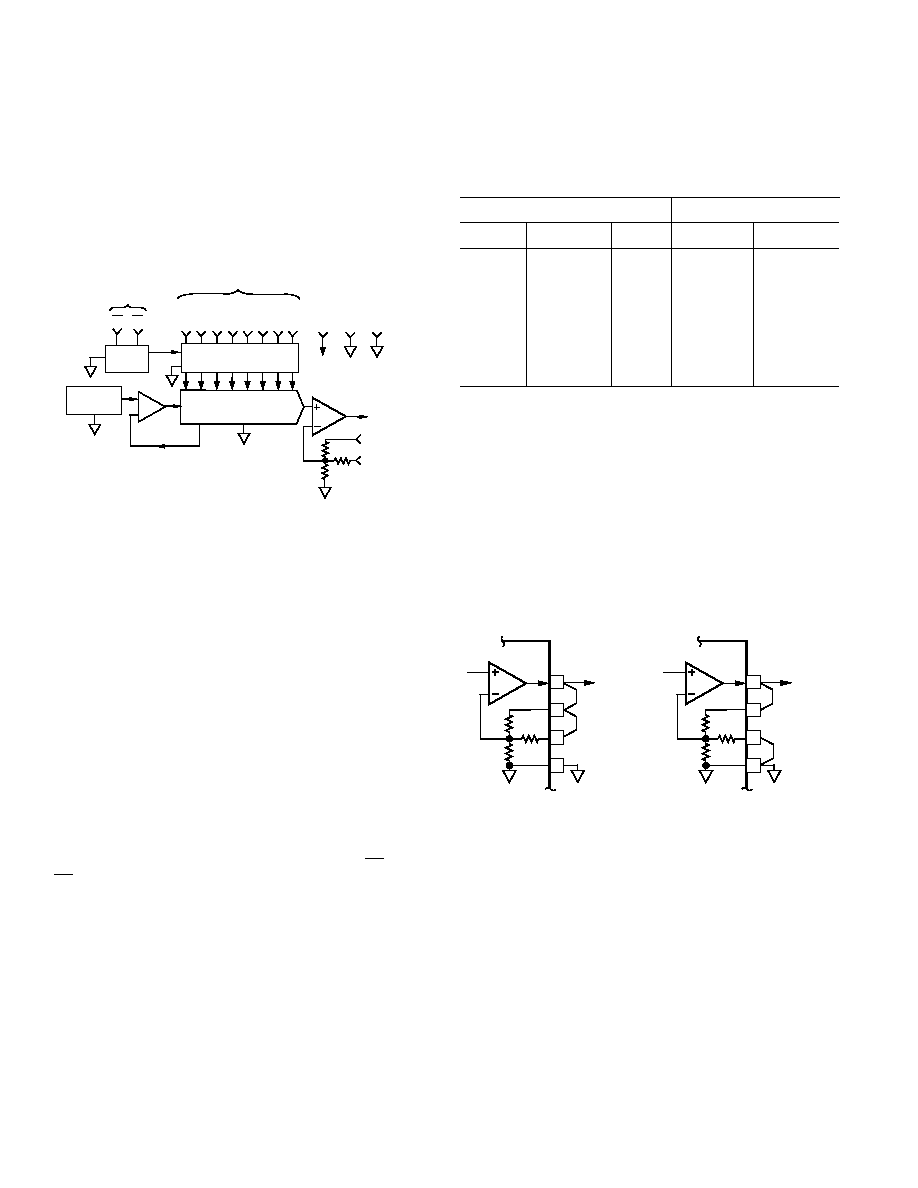
CIRCUIT DESCRIPTION
The AD558 consists of four major functional blocks, fabricated
on a single monolithic chip (see Figure 2). The main D-to-A
converter section uses eight equally-weighted laser-trimmed
current sources switched into a silicon-chromium thin-film
R/2R resistor ladder network to give a direct but unbuffered 0
mV to 400 mV output range. The transistors that form the
DAC switches are PNPs; this allows direct positive-voltage logic
interface and a zero-based output range.
CONTROL
AMP
BAND-
GAP
REFERENCE
OUTPUT
AMP
8-BIT VOLTAGE-SWITCHING
D-TO-A CONVERTER
I2L LATCHES
I2L
CONTROL
LOGIC
VOUT
SENSE
SELECT
+VCC
MSB
CS
CE
LSB
CONTROL
INPUTS
DB0
DB1
DB2
DB3
DB4
DB5
DB6
DB7
DIGITAL INPUT DATA
GND
Figure 2. AD558 Functional Block Diagram
The high speed output buffer amplifier is operated in the non-
inverting mode with gain determined by the user-connections
at the output range select pin. The gain-setting application
resistors are thin-film laser-trimmed to match and track the
DAC resistors and to assure precise initial calibration of the two
output ranges, 0 V to 2.56 V and 0 V to 10 V. The amplifier
output stage is an NPN transistor with passive pull-down for
zero-based output capability with a single power supply. The
internal precision voltage reference is of the patented bandgap
type. This design produces a reference voltage of 1.2 volts and
thus, unlike 6.3 volt temperature compensated Zeners, may be
operated from a single, low voltage logic power supply. The
microprocessor interface logic consists of an 8-bit data latch and
control circuitry. Low power, small geometry and high speed
are advantages of the I
2L design as applied to this section. I2L is
bipolar process compatible so that the performance of the ana-
log sections need not be compromised to provide on-chip logic
capabilities. The control logic allows the latches to be operated
from a decoded microprocessor address and write signal. If the
application does not involve a
P or data bus, wiring CS and
CE to ground renders the latches “transparent” for direct DAC
access.
MIL-STD-883
The rigors of the military/aerospace environment, temperature
extremes, humidity, mechanical stress, etc., demand the utmost
in electronic circuits. The AD558, with the inherent reliability
of integrated circuit construction, was designed with these ap-
plications in mind. The hermetically-sealed, low profile DIP
package takes up a fraction of the space required by equivalent
modular designs and protects the chip from hazardous environ-
ments. To further ensure reliability, military temperature range
AD558 grades S and T are available screened to MIL-STD-883.
For more complete data sheet information consult the Analog
Devices’ Military Databook.
CHIP AVAILABILITY
The AD558 is available in laser-trimmed, passivated chip form.
AD558J and AD558T chips are available. Consult the factory
for details.
Input Logic Coding
Digital Input Code
Output Voltage
Binary
Hexadecimal Decimal
2.56 V Range 10.000 V Range
0000 0000
00
0
0000 0001
01
1
0.010 V
0.039 V
0000 0010
02
2
0.020 V
0.078 V
0000 1111
0F
15
0.150 V
0.586 V
0001 0000
10
16
0.160 V
0.625 V
0111 1111
7F
127
1.270 V
4.961 V
1000 0000
80
128
1.280 V
5.000 V
1100 0000
C0
192
1.920 V
7.500 V
1111 1111
FF
255
2.55 V
9.961 V
CONNECTING THE AD558
The AD558 has been configured for ease of application. All ref-
erence, output amplifier and logic connections are made inter-
nally. In addition, all calibration trims are performed at the
factory assuring specified accuracy without user trims. The only
connection decision that must be made by the user is a single
jumper to select output voltage range. Clean circuit board lay-
out is facilitated by isolating all digital bit inputs on one side of
the package; analog outputs are on the opposite side.
Figure 3 shows the two alternative output range connections.
The 0 V to 2.56 V range may be selected for use with any power
supply between +4.5 V and +16.5 V. The 0 V to 10 V range
requires a power supply of +11.4 V to +16.5 V.
OUTPUT
AMP
16
15
14
13
GND
VOUT SELECT
VOUT SENSE
VOUT
OUTPUT
AMP
16
15
14
13
GND
VOUT SELECT
VOUT SENSE
VOUT
a. 0 V to 2.56 V Output Range b. 0 V to 10 V Output Range
Figure 3. Connection Diagrams
Because of its precise factory calibration, the AD558 is intended
to be operated without user trims for gain and offset; therefore
no provisions have been made for such user trims. If a small in-
crease in scale is required, however, it may be accomplished
by slightly altering the effective gain of the output buffer. A
resistor in series with VOUT SENSE will increase the output
range.
For example if a 0 V to 10.24 V output range is desired (40 mV
= 1 LSB), a nominal resistance of 850
is required. It must be
remembered that, although the internal resistors all ratio-
match and track, the absolute tolerance of these resistors is
typically
±20% and the absolute TC is typically –50 ppm/°C
(0 to –100 ppm/
°C). That must be considered when rescaling is
performed. Figure 4 shows the recommended circuitry for a
full-scale output range of 10.24 volts. Internal resistance values
shown are nominal.
相关PDF资料 |
PDF描述 |
|---|---|
| MS3450W28-21SZ | CONN RCPT 37POS WALL MNT W/SCKT |
| M83723/95R1808N | CONN PLUG 8POS STRAIGHT W/SCKT |
| AD5324BRMZ | IC DAC 12BIT QUAD VOUT 10-MSOP |
| MS3106E32-64S | CONN PLUG 54POS STRAIGHT W/SCKT |
| VE-B62-MV-F2 | CONVERTER MOD DC/DC 15V 150W |
相关代理商/技术参数 |
参数描述 |
|---|---|
| AD558JP | 功能描述:IC DAC 8BIT 5-15V IN MONO 20PLCC RoHS:否 类别:集成电路 (IC) >> 数据采集 - 数模转换器 系列:DACPORT® 产品培训模块:Data Converter Fundamentals DAC Architectures 标准包装:750 系列:- 设置时间:7µs 位数:16 数据接口:并联 转换器数目:1 电压电源:双 ± 功率耗散(最大):100mW 工作温度:0°C ~ 70°C 安装类型:表面贴装 封装/外壳:28-LCC(J 形引线) 供应商设备封装:28-PLCC(11.51x11.51) 包装:带卷 (TR) 输出数目和类型:1 电压,单极;1 电压,双极 采样率(每秒):143k |
| AD558JP-REEL | 制造商:Rochester Electronics LLC 功能描述: 制造商:Analog Devices 功能描述: |
| AD558JP-REEL7 | 功能描述:IC DAC 8BIT 5-15V IN MONO 20PLCC RoHS:否 类别:集成电路 (IC) >> 数据采集 - 数模转换器 系列:DACPORT® 产品培训模块:Data Converter Fundamentals DAC Architectures 标准包装:750 系列:- 设置时间:7µs 位数:16 数据接口:并联 转换器数目:1 电压电源:双 ± 功率耗散(最大):100mW 工作温度:0°C ~ 70°C 安装类型:表面贴装 封装/外壳:28-LCC(J 形引线) 供应商设备封装:28-PLCC(11.51x11.51) 包装:带卷 (TR) 输出数目和类型:1 电压,单极;1 电压,双极 采样率(每秒):143k |
| AD558JPZ | 功能描述:IC DAC 8BIT AMP/MCU 20-PLCC RoHS:是 类别:集成电路 (IC) >> 数据采集 - 数模转换器 系列:DACPORT® 产品培训模块:Data Converter Fundamentals DAC Architectures 标准包装:750 系列:- 设置时间:7µs 位数:16 数据接口:并联 转换器数目:1 电压电源:双 ± 功率耗散(最大):100mW 工作温度:0°C ~ 70°C 安装类型:表面贴装 封装/外壳:28-LCC(J 形引线) 供应商设备封装:28-PLCC(11.51x11.51) 包装:带卷 (TR) 输出数目和类型:1 电压,单极;1 电压,双极 采样率(每秒):143k |
| AD558JPZ-REEL7 | 功能描述:IC DAC 8BIT MONO 5-15V IN 20PLCC RoHS:是 类别:集成电路 (IC) >> 数据采集 - 数模转换器 系列:DACPORT® 标准包装:47 系列:- 设置时间:2µs 位数:14 数据接口:并联 转换器数目:1 电压电源:单电源 功率耗散(最大):55µW 工作温度:-40°C ~ 85°C 安装类型:表面贴装 封装/外壳:28-SSOP(0.209",5.30mm 宽) 供应商设备封装:28-SSOP 包装:管件 输出数目和类型:1 电流,单极;1 电流,双极 采样率(每秒):* |
发布紧急采购,3分钟左右您将得到回复。