- 您现在的位置:买卖IC网 > PDF目录8912 > AD5611AKSZ-500RL7 (Analog Devices Inc)IC DAC 10BIT BUFF V-OUT SC70-6 PDF资料下载
参数资料
| 型号: | AD5611AKSZ-500RL7 |
| 厂商: | Analog Devices Inc |
| 文件页数: | 8/24页 |
| 文件大小: | 0K |
| 描述: | IC DAC 10BIT BUFF V-OUT SC70-6 |
| 产品培训模块: | Data Converter Fundamentals DAC Architectures |
| 标准包装: | 1 |
| 系列: | nanoDAC™ |
| 设置时间: | 6µs |
| 位数: | 10 |
| 数据接口: | DSP,MICROWIRE?,QSPI?,串行,SPI? |
| 转换器数目: | 1 |
| 电压电源: | 单电源 |
| 功率耗散(最大): | 500µW |
| 工作温度: | -40°C ~ 125°C |
| 安装类型: | 表面贴装 |
| 封装/外壳: | 6-TSSOP,SC-88,SOT-363 |
| 供应商设备封装: | SC-70-6 |
| 包装: | 标准包装 |
| 输出数目和类型: | 1 电压,单极;1 电压,双极 |
| 其它名称: | AD5611AKSZ-500RL7DKR |
AD5601/AD5611/AD5621
Data Sheet
Rev. G | Page 16 of 24
POWER-ON RESET
The AD5601/AD5611/AD5621 contain a power-on reset circuit
that controls the output voltage during power-up. The DAC
register is filled with 0s and the output voltage is 0 V. It remains
there until a valid write sequence is made to the DAC. This is
useful in applications in which it is important to know the state
of the DAC output while it is in the process of powering up.
POWER-DOWN MODES
The AD5601/AD5611/AD5621 have four separate modes of
operation. These modes are software-programmable by setting
two bits (DB15 and DB14) in the control register. Table 6 shows
how the state of the bits corresponds to the operating mode of
the device.
Table 6. Operating Modes of the AD5601/AD5611/AD5621
DB15
DB14
Operating Mode
0
Normal operation
Power-down modes:
0
1
1 kΩ to GND
1
0
100 kΩ to GND
1
Three-state
When both bits are set to 0, the part has normal power
consumption of 100 A maximum at 5 V. However, for the
three power-down modes, the supply current falls to typically
0.2 A at 3 V.
Not only does the supply current fall, but the output stage is
also internally switched from the output of the amplifier to a
resistor network of known values. This has the advantage that
the output impedance of the part is known while the part is in
power-down mode.
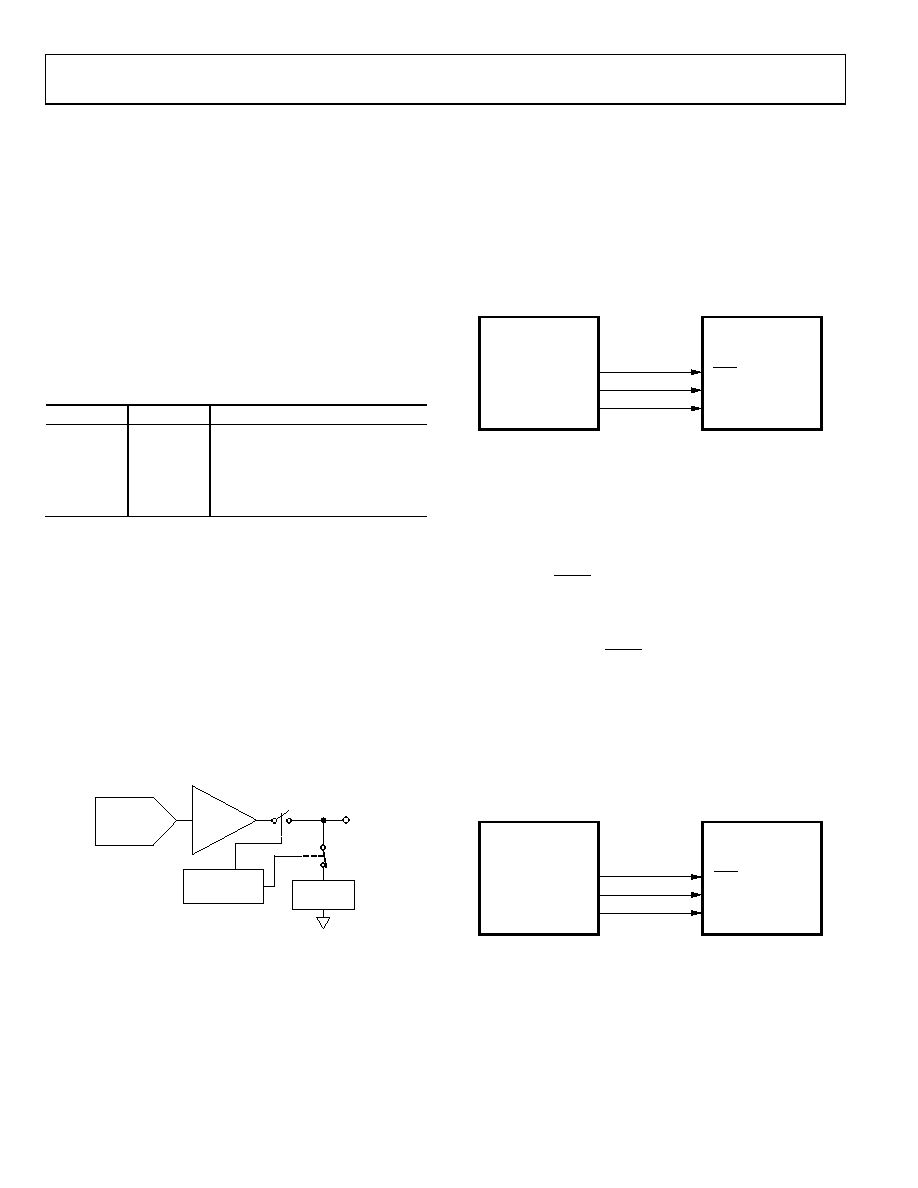
There are three different options: the output is connected
internally to GND through a 1 k resistor or a 100 k resistor,
or the output is left open-circuited (three-stated). Figure 45
shows the output stage.
Figure 45. Output Stage During Power-Down
The bias generator, output amplifier, resistor string, and other
associated linear circuitry are all shut down when power-down
mode is activated. However, the contents of the DAC register
are unaffected when in power-down. The time to exit power-
down is typically 13 s for VDD = 5 V and 16 s for VDD = 3 V.
See Figure 21 for a plot.
MICROPROCESSOR INTERFACING
AD5601/AD5611/AD5621 to ADSP-2101 Interface
Figure 46 shows a serial interface between the AD5601/
AD5611/AD5621 and the ADSP-2101. The ADSP-2101 should
be set up to operate in SPORT transmit alternate framing mode.
The ADSP-2101 SPORT is programmed through the SPORT
control register and should be configured as follows: internal
clock operation, active low framing, and 16-bit word length.
Transmission is initiated by writing a word to the Tx register
after the SPORT is enabled.
Figure 46. AD5601/AD5611/AD5621 to ADSP-2101 Interface
AD5601/AD5611/AD5621 to 68HC11/68L11 Interface
Figure 47 shows a serial interface between the AD5601/AD5611/
AD5621 and the 68HC11/68L11 microcontroller. SCK of the
68HC11/68L11 drives the SCLK of the AD5601/AD5611/
AD5621, while the MOSI output drives the serial data line of
the DAC. The SYNC signal is derived from a port line (PC7).
The setup conditions for correct operation of this interface are
as follows: the 68HC11/68L11 should be configured so that the
CPOL bit is 0 and the CPHA bit is 1. When data is being trans-
mitted to the DAC, the SYNC line is taken low (PC7). When the
68HC11/68L11 are configured as indicated, data appearing on
the MOSI output is valid on the falling edge of SCK. Serial data
from the 68HC11/68L11 is transmitted in 8-bit bytes with only
eight falling clock edges occurring in the transmit cycle. Data is
transmitted MSB first. To load data to the AD5601/AD5611/
AD5621, PC7 is left low after the first eight bits are transferred
and a second serial write operation is performed to the DAC.
PC7 is taken high at the end of this procedure.
Figure 47. AD5601/AD5611/AD5621 to 68HC11/68L11 Interface
POWER-DOWN
CIRCUITRY
RESISTOR
NETWORK
VOUT
RESISTOR
STRING DAC
AMPLIFIER
06853-
044
AD5601/AD5611/
AD5621*
*ADDITIONAL PINS OMITTED FOR CLARITY
TFS
DT
SCLK
SYNC
SDIN
SCLK
06853-
045
ADSP-2101*
68HC11/
68L11*
AD5601/AD5611/
AD5621*
*ADDITIONAL PINS OMITTED FOR CLARITY
PC7
SCK
MOSI
SYNC
SCLK
SDIN
06853-
046
相关PDF资料 |
PDF描述 |
|---|---|
| 74AVCH4T245DGVRG4 | IC BUS TRANSCVR 4BIT 16TVSOP |
| GTC00AF-32-76P | CONN RCPT 19POS WALL MNT W/PINS |
| VE-J6N-MZ-F1 | CONVERTER MOD DC/DC 18.5V 25W |
| 74AVCH4T245PWRE4 | IC BUS TRANSCVR 4BIT 16TSSOP |
| M83723/75G1005N | CONN PLUG 5POS STRAIGHT W/SCKT |
相关代理商/技术参数 |
参数描述 |
|---|---|
| AD5611AKSZ-REEL7 | 功能描述:IC DAC 10BIT BUFF V-OUT SC70-6 RoHS:是 类别:集成电路 (IC) >> 数据采集 - 数模转换器 系列:nanoDAC™ 产品培训模块:Data Converter Fundamentals DAC Architectures 设计资源:Unipolar, Precision DC Digital-to-Analog Conversion using AD5450/1/2/3 8-14-Bit DACs (CN0052) Precision, Bipolar, Configuration for AD5450/1/2/3 8-14bit Multiplying DACs (CN0053) AC Signal Processing Using AD5450/1/2/3 Current Output DACs (CN0054) Programmable Gain Element Using AD5450/1/2/3 Current Output DAC Family (CN0055) Single Supply Low Noise LED Current Source Driver Using a Current Output DAC in the Reverse Mode (CN0139) 标准包装:10,000 系列:- 设置时间:- 位数:12 数据接口:DSP,MICROWIRE?,QSPI?,串行,SPI? 转换器数目:1 电压电源:单电源 功率耗散(最大):- 工作温度:-40°C ~ 125°C 安装类型:表面贴装 封装/外壳:SOT-23-8 薄型,TSOT-23-8 供应商设备封装:TSOT-23-8 包装:带卷 (TR) 输出数目和类型:1 电流,单极;1 电流,双极 采样率(每秒):2.7M |
| AD5611BKS | 制造商:AD 制造商全称:Analog Devices 功能描述:2.7 V to 5.5 V, <100 UA, 8-/10-/12-Bit nanoDAC D/A, SPI Interface, SC70 Package |
| AD5611BKSZ | 制造商:Analog Devices 功能描述:DAC 8BIT +/-0.5LSB 5.5VIN 6SC70 制造商:Analog Devices 功能描述:DAC, 8BIT, +/-0.5LSB, 5.5VIN, 6SC70 制造商:Analog Devices 功能描述:DAC, 8BIT, +/-0.5LSB, 5.5VIN, 6SC70; Resolution (Bits):10bit; Input Channel Type:Serial; Supply Voltage Range:2.7V to 5.5V; Digital IC Case Style:TSSOP; No. of Pins:6; Data Interface:Microwire, QSPI, SPI; Supply Current:75A; ;RoHS Compliant: Yes |
| AD5611BKSZ-500RL7 | 功能描述:IC DAC 10BIT SPI 5V SC70-6 RoHS:是 类别:集成电路 (IC) >> 数据采集 - 数模转换器 系列:nanoDAC™ 产品培训模块:Data Converter Fundamentals DAC Architectures 设计资源:Unipolar, Precision DC Digital-to-Analog Conversion using AD5450/1/2/3 8-14-Bit DACs (CN0052) Precision, Bipolar, Configuration for AD5450/1/2/3 8-14bit Multiplying DACs (CN0053) AC Signal Processing Using AD5450/1/2/3 Current Output DACs (CN0054) Programmable Gain Element Using AD5450/1/2/3 Current Output DAC Family (CN0055) Single Supply Low Noise LED Current Source Driver Using a Current Output DAC in the Reverse Mode (CN0139) 标准包装:10,000 系列:- 设置时间:- 位数:12 数据接口:DSP,MICROWIRE?,QSPI?,串行,SPI? 转换器数目:1 电压电源:单电源 功率耗散(最大):- 工作温度:-40°C ~ 125°C 安装类型:表面贴装 封装/外壳:SOT-23-8 薄型,TSOT-23-8 供应商设备封装:TSOT-23-8 包装:带卷 (TR) 输出数目和类型:1 电流,单极;1 电流,双极 采样率(每秒):2.7M |
| AD5611BKSZ-REEL7 | 功能描述:IC DAC 10BIT SGL 2.7-5.5V SC70-6 RoHS:是 类别:集成电路 (IC) >> 数据采集 - 数模转换器 系列:nanoDAC™ 产品培训模块:Data Converter Fundamentals DAC Architectures 标准包装:3,000 系列:nanoDAC™ 设置时间:80µs 位数:18 数据接口:DSP,MICROWIRE?,QSPI?,串行,SPI? 转换器数目:1 电压电源:单电源 功率耗散(最大):- 工作温度:-40°C ~ 105°C 安装类型:表面贴装 封装/外壳:SOT-23-8 供应商设备封装:SOT-23-8 包装:带卷 (TR) 输出数目和类型:1 电压,单极 采样率(每秒):- 产品目录页面:784 (CN2011-ZH PDF) 配用:EVAL-AD5680EBZ-ND - BOARD EVAL FOR AD5680 其它名称:AD5680BRJZ-2REEL7TR |
发布紧急采购,3分钟左右您将得到回复。