参数资料
| 型号: | AD561KNZ |
| 厂商: | Analog Devices Inc |
| 文件页数: | 7/8页 |
| 文件大小: | 0K |
| 描述: | IC DAC 10BIT MONO VOLT IN 16DIP |
| 产品培训模块: | Data Converter Fundamentals DAC Architectures |
| 标准包装: | 1 |
| 设置时间: | 250ns |
| 位数: | 10 |
| 数据接口: | 并联 |
| 转换器数目: | 1 |
| 电压电源: | 双 ± |
| 工作温度: | 0°C ~ 70°C |
| 安装类型: | 通孔 |
| 封装/外壳: | 16-DIP(0.300",7.62mm) |
| 供应商设备封装: | 16-PDIP |
| 包装: | 管件 |
| 输出数目和类型: | 1 电流,单极;1 电流,双极 |
| 采样率(每秒): | * |
AD561
–7–
REV. A
Fastest operation will be obtained by minimizing lead lengths,
stray capacitance and impedance levels. Both supplies should be
bypassed near the devices; 0.1
F will be sufficient since the
AD561 runs at constant supply current regardless of input code.
POWER SUPPLY SELECTION
The AD561 will operate over a wide range of power supply
voltages, with a total supply from 15.3 to 33 volts. Symmetrical
supplies are not required, and in many applications not recom-
mended. Maximum allowable supplies are
±16.5 V.
The positive supply level determines the digital threshold level,
as explained on page 6 and shown in Figure 6. It is therefore
recommended that VCC be connected directly to the digital
supply for best threshold match.
Positive output voltage compliance range is unaffected by the
positive supply level because of the open collector output stage
design; thus the full +10 volt compliance is available even with a
+5 volt VCC level. Power supply rejection is excellent, so that
digital supply noise will not be reflected to the output. but use
of a 0.1
F bypass capacitor near the AD561 is recommended
for decoupling.
The nominal negative supply level is –15 volts, with an allow-
able range of –10.8 to –16.5 volts. The negative supply level
affects the negative compliance range, as shown in Figure 7.
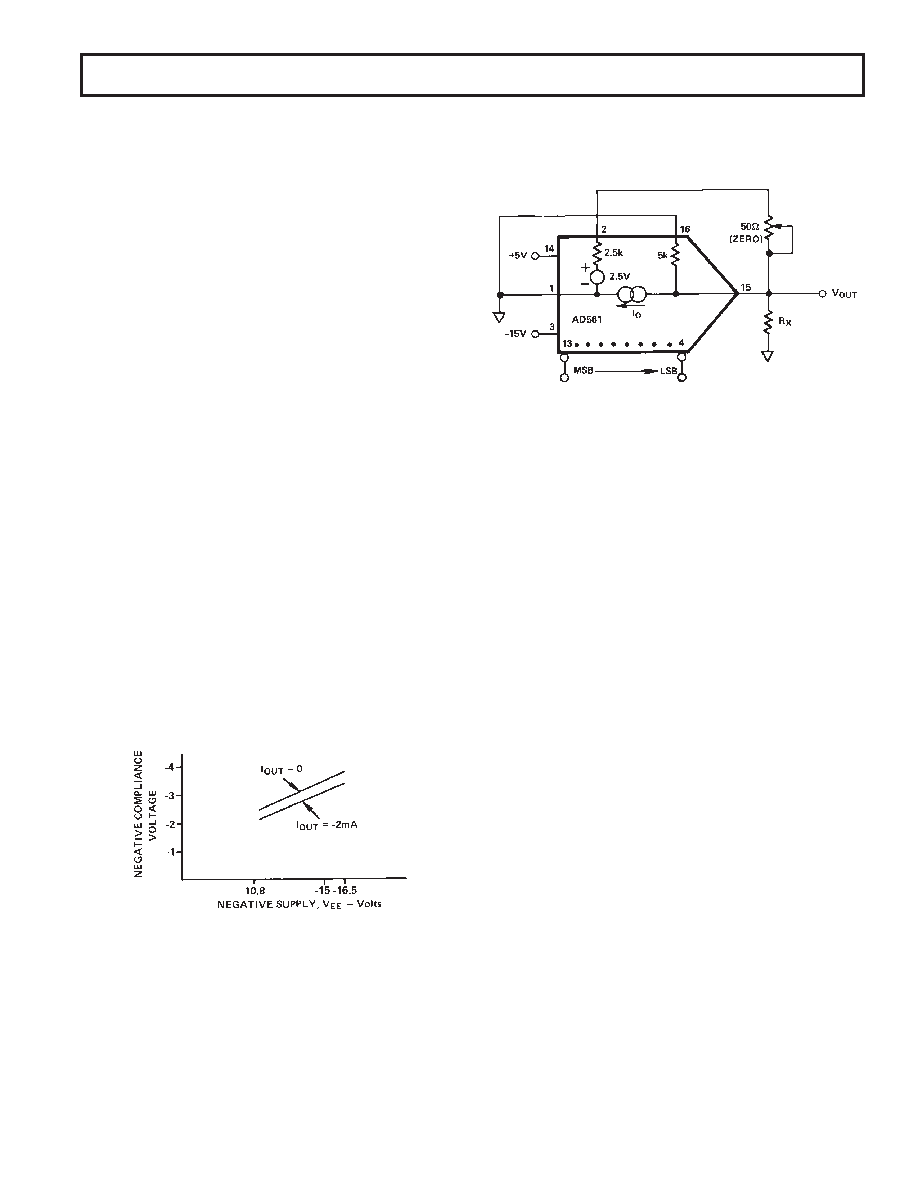
OUTPUT VOLTAGE COMPLIANCE
The AD561 has a typical output compliance range from –3 to
+10 volts. The output current is unaffected by changes in the
output terminal voltage over that range. This results from the
use of open collector output switching stages in a cascade
configuration, and gives an output impedance of 40 M
.
Positive compliance range is limited only by collector break-
down (and is independent of positive supply level), but the
negative range is limited by the required bias levels and resistor
ladder voltage. Negative compliance varies with negative supply,
as shown in Figure 7. The compliance range is guaranteed to be
–2 to +10 volts with VEE = –15 volts.
Figure 7. Typical Negative Compliance Range vs.
Negative Supply
DIRECT UNBUFFERED VOLTAGE OUTPUT
The wide compliance range allows direct current-to-voltage
conversion with just an output resistor. Figure 8 shows a
connection using the gain and bipolar output resistors to give a
±1.66 volt bipolar swing. In this situation, the digital code is
complementary binary. Other combinations of internal and
external output resistors (RX) can be used to scale to alternate
voltage ranges, simply by appropriately scaling the 0 to –2 mA
unipolar output current and using the 2.5 volt reference voltage
for bipolar offset. For example, setting RX = 2.5 k gives a ± 1
volt range with a 1 k
equivalent output impedance. A 0 to +10
volt output can be obtained by connecting the 5 k
gain resistor
to 9.99 volts; again the digital code is complementary binary.
Figure 8. Unbuffered Bipolar Voltage Output
HIGH SPEED 10-BIT A/D CONVERTERS
The fast settling characteristics of the AD561 make it ideal for
high speed successive approximation A/D converters. The
internal reference and trimmed application resistors allow a
10-bit converter system to be constructed with a minimum parts
count. Shown here is a configuration using standard compo-
nents; this system completes a full 10-bit conversion in 5.5
s
unipolar or 12
s bipolar. This converter will be accurate to
±1/2 LSB of 10 bits and have a typical gain TC of 10 ppm/°C.
In the unipolar mode, the system range is 0 to 9.99 volts,
with each bit having a value of 9.76 mV. For true conversion
accuracy, an A/D converter should be trimmed so that a given
bit code output results from input levels from 1/2 LSB below to
1/2 LSB above the exact voltage which that code represents.
Therefore, the converter zero point should be trimmed with an
input voltage of +4.9 mV; trim R1 until the LSB just begins to
appear in the output code (all other bits “0”). For full scale, use
an input voltage of +9.985 volts (10 volts – 1 LSB – 1/2 LSB);
then trim R2 again until the LSB just begins to appear (all other
bits “1”).
The bipolar signal range is –5.0 to +4.99 volts. Bipolar offset
trimming is done by applying a +4.9 mV input signal and
trimming R1 for the LSB transition (MSB “1,” all other bits
“0.”) Full scale is set by applying –4.995 volts and trimming R2
for the LSB transition (all other bits “0”). In many applications,
the pretrimmed application resistors are sufficiently accurate
that external trimmers will be unnecessary, especially in
situations requiring less than full 10-bit
± 1/2 LSB accuracy.
For fastest operation, the impedance at the comparator sum-
ming node must be minimized, as mentioned in the section on
settling time. However, lowering the impedance will reduce the
voltage signal to the comparator (at an equivalent impedance of
1 k
, 1 LSB = 2 mV) to the point that comparator performance
will be sacrificed. A 1 k
resistor is the optimum value for this
application for 10-bit accuracy. The chart shown in the figure
gives the speed of the ADC for
±1/2 LSB accuracy (and no
missing codes) for 6-, 8- and 10-bit resolution.
相关PDF资料 |
PDF描述 |
|---|---|
| VE-J54-MZ-B1 | CONVERTER MOD DC/DC 48V 25W |
| VI-JWK-MZ-B1 | CONVERTER MOD DC/DC 40V 25W |
| AD7228KN | IC DAC 8BIT OCTAL W/AMP 24-DIP |
| VI-JWH-MZ-B1 | CONVERTER MOD DC/DC 52V 25W |
| VI-JWF-MZ-B1 | CONVERTER MOD DC/DC 72V 25W |
相关代理商/技术参数 |
参数描述 |
|---|---|
| AD561S | 制造商:AD 制造商全称:Analog Devices 功能描述:Low Cost 10-Bit Monolithic D/A Converter |
| AD561SD | 功能描述:数模转换器- DAC IC MONO 10-BIT D/A CONV RoHS:否 制造商:Texas Instruments 转换器数量:1 DAC 输出端数量:1 转换速率:2 MSPs 分辨率:16 bit 接口类型:QSPI, SPI, Serial (3-Wire, Microwire) 稳定时间:1 us 最大工作温度:+ 85 C 安装风格:SMD/SMT 封装 / 箱体:SOIC-14 封装:Tube |
| AD561SD/883B | 制造商:Analog Devices 功能描述:DAC 1-CH R-2R 10-bit 16-Pin CDIP Tube 制造商:Analog Devices 功能描述:DAC 1CH R-2R 10-BIT 16CDIP - Rail/Tube 制造商:Rochester Electronics LLC 功能描述:IC, MONO 10-BIT D/A CONV - Bulk 制造商:Analog Devices Inc. 功能描述:Digital to Analog Converters - DAC IC MONO 10-BIT D/A CONV 制造商:Analog Devices Inc. 功能描述:Digital to Analog Converters - DAC Low Cost 10-Bit Monolithic 制造商:Analog Devices 功能描述:CONVERTER - DAC |
| AD561SD-883B | 制造商:AD 制造商全称:Analog Devices 功能描述:Low Cost 10-Bit Monolithic D/A Converter |
| AD561T | 制造商:AD 制造商全称:Analog Devices 功能描述:Low Cost 10-Bit Monolithic D/A Converter |
发布紧急采购,3分钟左右您将得到回复。