参数资料
| 型号: | AD5623RBRMZ-3 |
| 厂商: | Analog Devices Inc |
| 文件页数: | 15/32页 |
| 文件大小: | 0K |
| 描述: | IC DAC NANO 12BIT DUAL 10-MSOP |
| 产品培训模块: | Data Converter Fundamentals DAC Architectures |
| 标准包装: | 50 |
| 系列: | nanoDAC™ |
| 设置时间: | 3µs |
| 位数: | 12 |
| 数据接口: | 串行 |
| 转换器数目: | 2 |
| 电压电源: | 单电源 |
| 功率耗散(最大): | 5mW |
| 工作温度: | -40°C ~ 105°C |
| 安装类型: | 表面贴装 |
| 封装/外壳: | 10-TFSOP,10-MSOP(0.118",3.00mm 宽) |
| 供应商设备封装: | 10-MSOP |
| 包装: | 管件 |
| 输出数目和类型: | 2 电压,单极;2 电压,双极 |
| 采样率(每秒): | 287k |
| 产品目录页面: | 783 (CN2011-ZH PDF) |
第1页第2页第3页第4页第5页第6页第7页第8页第9页第10页第11页第12页第13页第14页当前第15页第16页第17页第18页第19页第20页第21页第22页第23页第24页第25页第26页第27页第28页第29页第30页第31页第32页
AD5623R/AD5643R/AD5663R
Data Sheet
Rev. E | Page 22 of 32
POWER-ON RESET
The AD5623R/AD5643R/AD5663R contain a power-on reset
circuit that controls the output voltage during power-up. The
AD5623R/AD5643R/AD5663R DACs output power up to 0 V,
and the output remains there until a valid write sequence is
made to the DACs. This is useful in applications where it is
important to know the state of the output of the DACs while
they are in the process of powering up. Any events on LDAC or
CLR during power-on reset are ignored.
SOFTWARE RESET
The AD5623R/AD5643R/AD5663R contain a software reset
function. Command 101 is reserved for the software reset
function (see Table 8). The software reset command contains
two reset modes that are software-programmable by setting bit
DB0 in the control register. Table 10 shows how the state of the
bit corresponds to the mode of operation of the device. Table 12
shows the contents of the input shift register during the
software reset mode of operation.
Table 10. Software Reset Modes
DB0
Registers Reset to Zero
0
DAC register
Input register
1 (Power-on Reset)
DAC register
Input register
LDAC register
Power-down register
Internal reference setup register
POWER-DOWN MODES
The AD5623R/AD5643R/AD5663R contain four separate
modes of operation. Command 100 is reserved for the power-
down function (see Table 8). These modes are software-
programmable by setting Bit DB5 and Bit DB4 in the control
register. Table 11 shows how the state of the bits corresponds to
the mode of operation of the device. Any or all DACs (DAC B
and DAC A) can be powered down to the selected mode by
setting the corresponding two bits (Bit DB1 and Bit DB0) to 1.
By executing the same Command 100, any combination of DACs
can be powered up by setting Bit DB5 and Bit DB4 to normal
operation mode.
Again, to select which combination of DAC channels to power
up, set the corresponding bits (Bit DB1 and Bit DB0) to 1. See
Table 13 for contents of the input shift register during power-
down/power-up operation.
The DAC output powers up to the value in the input register
while LDAC is low. If LDAC is high, the DAC ouput powers up
to the value held in the DAC register before power-down.
Table 11. Modes of Operation
DB5
DB4
Operating Mode
0
Normal operation
Power-down modes
0
1
1 kΩ to GND
1
0
100 kΩ to GND
1
Three-state
When both Bit DB1 and Bit DB2 are set to 0, the part works
normally, with its normal power consumption of 250 A at 5 V.
However, for the three power-down modes, the supply current
falls to 480 nA at 5 V (200 nA at 3 V). Not only does the supply
current fall, but the output stage is also internally switched from
the output of the amplifier to a resistor network of known values.
This has the advantage that the output impedance of the part is
known while the part is in power-down mode. The outputs can
either be connected internally to GND through a 1 k or 100 k
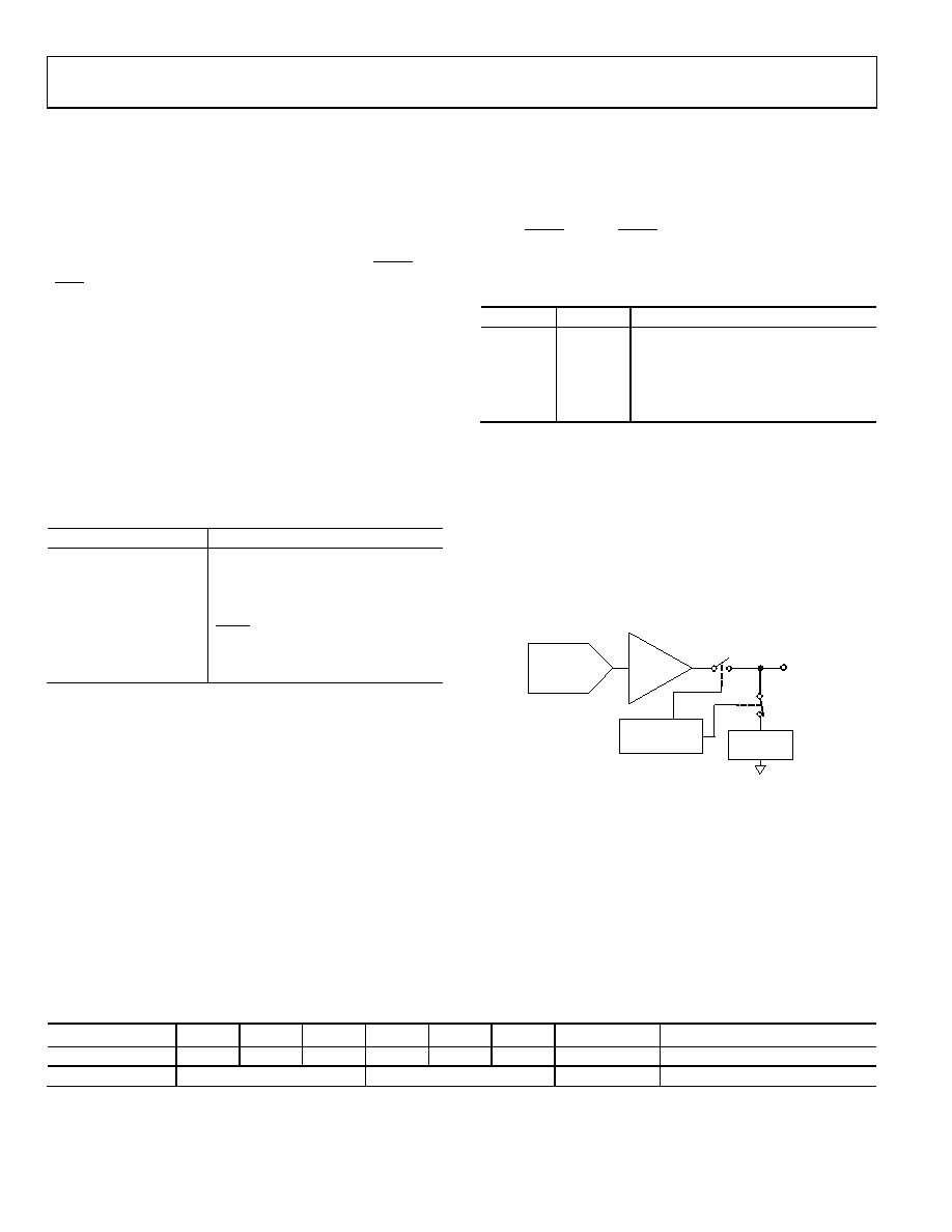
resistor or left open-circuited (three-state) (see Figure 55).
RESISTOR
NETWORK
VOUT
RESISTOR
STRING DAC
POWER-DOWN
CIRCUITRY
AMPLIFIER
05858-
036
Figure 55. Output Stage During Power-Down
The bias generator, the output amplifier, the resistor string,
and other associated linear circuitry are shut down when
power-down mode is activated. However, the contents of the
DAC register are unaffected when in power-down. The time
to exit power-down is typically 4 s for both VDD = 5 V and
VDD = 3 V (see Figure 37).
Table 12. 24-Bit Input Shift Register Contents for Software Reset Command
MSB
LSB
DB23 to DB22
DB21
DB20
DB19
DB18
DB17
DB16
DB15 to DB1
DB0
x
1
0
1
x
1/0
Don’t care
Command bits (C2 to C0)
Address bits (A2 to A0)
Don’t care
Determines software reset mode
相关PDF资料 |
PDF描述 |
|---|---|
| VE-BNX-MV-F1 | CONVERTER MOD DC/DC 5.2V 150W |
| VI-201-MY-F2 | CONVERTER MOD DC/DC 12V 50W |
| AD5623RBRMZ-5 | IC DAC NANO 12BIT DUAL 10-MSOP |
| MS3454W14S-7PW | CONN RCPT 3POS JAM NUT W/PINS |
| AD5312BRMZ | IC DAC 10BIT DUAL R-R 10-MSOP |
相关代理商/技术参数 |
参数描述 |
|---|---|
| AD5623RBRMZ-3REEL7 | 功能描述:IC DAC NANO 12BIT DUAL 10-MSOP RoHS:是 类别:集成电路 (IC) >> 数据采集 - 数模转换器 系列:nanoDAC™ 产品培训模块:LTC263x 12-, 10-, and 8-Bit VOUT DAC Family 特色产品:LTC2636 - Octal 12-/10-/8-Bit SPI VOUT DACs with 10ppm/°C Reference 标准包装:91 系列:- 设置时间:4µs 位数:10 数据接口:MICROWIRE?,串行,SPI? 转换器数目:8 电压电源:单电源 功率耗散(最大):2.7mW 工作温度:-40°C ~ 85°C 安装类型:表面贴装 封装/外壳:14-WFDFN 裸露焊盘 供应商设备封装:14-DFN-EP(4x3) 包装:管件 输出数目和类型:8 电压,单极 采样率(每秒):* |
| AD5623RBRMZ-5 | 功能描述:IC DAC NANO 12BIT DUAL 10-MSOP RoHS:是 类别:集成电路 (IC) >> 数据采集 - 数模转换器 系列:nanoDAC™ 产品培训模块:Lead (SnPb) Finish for COTS Obsolescence Mitigation Program 标准包装:50 系列:- 设置时间:4µs 位数:12 数据接口:串行 转换器数目:2 电压电源:单电源 功率耗散(最大):- 工作温度:-40°C ~ 85°C 安装类型:表面贴装 封装/外壳:8-TSSOP,8-MSOP(0.118",3.00mm 宽) 供应商设备封装:8-uMAX 包装:管件 输出数目和类型:2 电压,单极 采样率(每秒):* 产品目录页面:1398 (CN2011-ZH PDF) |
| AD5623RBRMZ-5REEL7 | 功能描述:IC DAC NANO 12BIT DUAL 10-MSOP RoHS:是 类别:集成电路 (IC) >> 数据采集 - 数模转换器 系列:nanoDAC™ 产品培训模块:LTC263x 12-, 10-, and 8-Bit VOUT DAC Family 特色产品:LTC2636 - Octal 12-/10-/8-Bit SPI VOUT DACs with 10ppm/°C Reference 标准包装:91 系列:- 设置时间:4µs 位数:10 数据接口:MICROWIRE?,串行,SPI? 转换器数目:8 电压电源:单电源 功率耗散(最大):2.7mW 工作温度:-40°C ~ 85°C 安装类型:表面贴装 封装/外壳:14-WFDFN 裸露焊盘 供应商设备封装:14-DFN-EP(4x3) 包装:管件 输出数目和类型:8 电压,单极 采样率(每秒):* |
| AD5624 | 制造商:AD 制造商全称:Analog Devices 功能描述:2.7 V to 5.5 V, 450 レA, Rail-to-Rail Output, Quad, 12-/16-Bit nanoDACs |
| AD5624BCPZ-250RL7 | 制造商:AD 制造商全称:Analog Devices 功能描述:2.7 V to 5.5 V, 450 レA, Rail-to-Rail Output, Quad, 12-/16-Bit nanoDACs |
发布紧急采购,3分钟左右您将得到回复。