- 您现在的位置:买卖IC网 > PDF目录8661 > AD5624BCPZ-R2 (Analog Devices Inc)IC DAC NANO 12BIT QUAD 10-LFCSP PDF资料下载
参数资料
| 型号: | AD5624BCPZ-R2 |
| 厂商: | Analog Devices Inc |
| 文件页数: | 8/24页 |
| 文件大小: | 0K |
| 描述: | IC DAC NANO 12BIT QUAD 10-LFCSP |
| 产品培训模块: | Data Converter Fundamentals DAC Architectures |
| 标准包装: | 1 |
| 系列: | nanoDAC™ |
| 设置时间: | 3µs |
| 位数: | 12 |
| 数据接口: | DSP,MICROWIRE?,QSPI?,串行,SPI? |
| 转换器数目: | 4 |
| 电压电源: | 单电源 |
| 工作温度: | -40°C ~ 105°C |
| 安装类型: | 表面贴装 |
| 封装/外壳: | 10-WFDFN 裸露焊盘,CSP |
| 供应商设备封装: | 10-LFCSP-WD(3x3) |
| 包装: | 标准包装 |
| 输出数目和类型: | 4 电压,单极;4 电压,双极 |
| 采样率(每秒): | 287k |
| 其它名称: | AD5624BCPZ-R2DKR |
AD5624/AD5664
Rev. 0 | Page 16 of 24
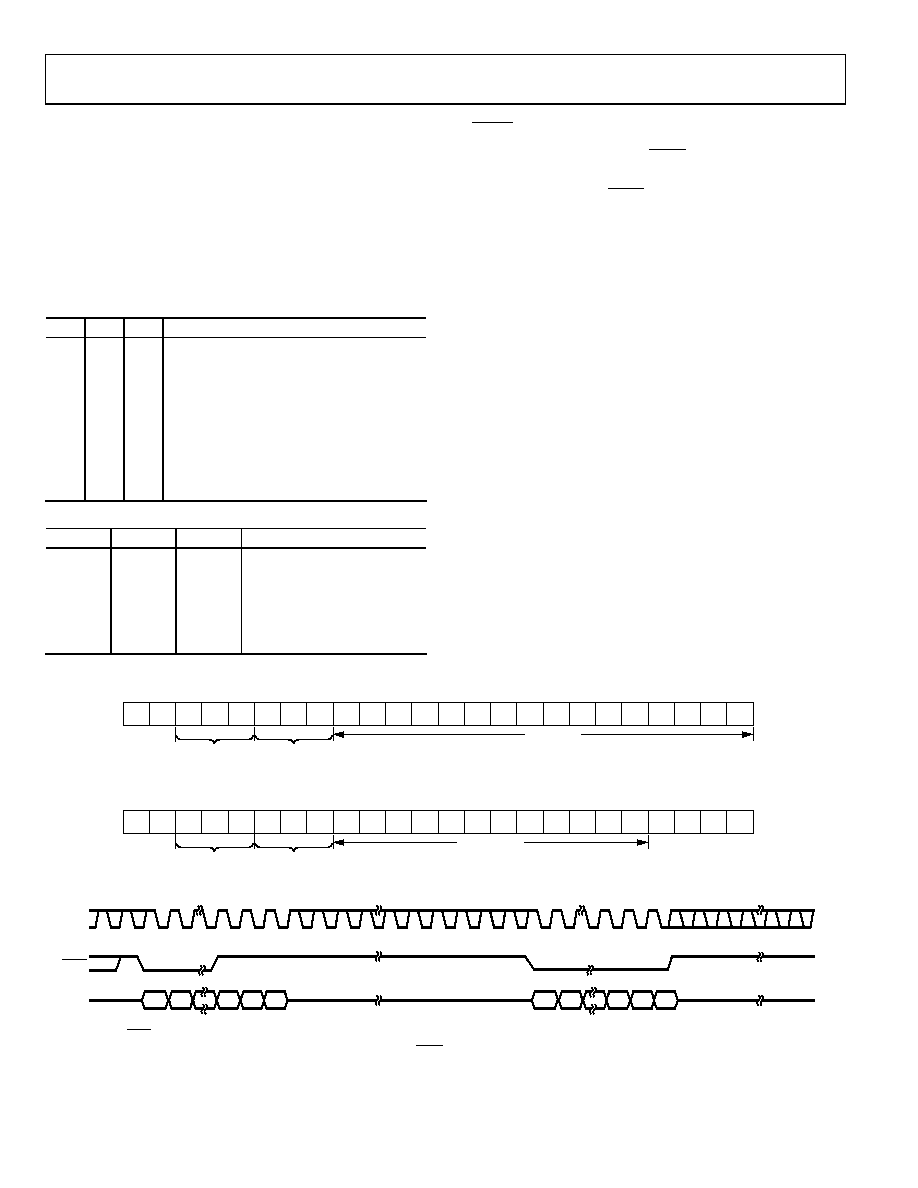
INPUT SHIFT REGISTER
The input shift register is 24 bits wide The first two bits are
don’t care bits. The next three bits are the Command bits, C2 to
C0 (see Table 7), followed by the 3-bit DAC address, A2 to A0
(see Table 8), and then the 16-, 12-bit data-word. The data-word
comprises the 16-, 12- bit input code followed by 0 or 4 don’t
care bits for the AD5664 and AD5624 respectively (see Figure
31 and Figure 32). These data bits are transferred to the DAC
register on the 24th falling edge of SCLK.
Table 7. Command Definition
C2
C1
C0
Command
0
Write to input register n
0
1
Update DAC register n
0
1
0
Write to input register n, update all
(software LDAC)
0
1
Write to and update DAC channel n
1
0
Power down DAC (power-up)
1
0
1
Reset
1
0
Load LDAC register
1
Reserved
Table 8. Address Command
A2
A1
A0
ADDRESS (n)
0
DAC A
0
1
DAC B
0
1
0
DAC C
0
1
DAC D
1
All DACs
SYNC INTERRUPT
In a normal write sequence, the SYNC line is kept low for at least
24 falling edges of SCLK, and the DAC is updated on the 24th
falling edge. However, if SYNC is brought high before the 24
th
falling edge, then this acts as an interrupt to the write sequence.
The input shift register is reset and the write sequence is seen as
invalid. Neither an update of the DAC register contents nor a
change in the operating mode occurs (see Figure 33).
POWER-ON RESET
The AD5624/AD5664 family contains a power-on reset circuit
that controls the output voltage during power-up. The AD5624/
AD5664 DAC outputs power up to 0 V and the output remains
there until a valid write sequence is made to the DAC. This is
useful in applications where it is important to know the state of
the output of the DAC while it is in the process of powering up.
X
C2
C1
C0
A2
A1
A0
D15 D14 D13 D12 D11 D10
D9
D8
D7
D6
D5
D4
D3
D2
D1
D0
DB23 (MSB)
DB0 (LSB)
COMMAND BITS
ADDRESS BITS
DATA BITS
05
94
3-
03
4
Figure 31. AD5664 Input Shift Register Contents
X
C2
C1
C0
A2
A1
A0
XXX
X
D11 D10
D9
D8
D7
D6
D5
D4
D3
D2
D1
D0
DB23 (MSB)
DB0 (LSB)
COMMAND BITS
ADDRESS BITS
DATA BITS
05
94
3-
03
5
Figure 32. AD5624 Input Shift Register Contents
DIN
DB23
DB0
VALID WRITE SEQUENCE, OUTPUT UPDATES
ON THE 24TH FALLING EDGE
SYNC
SCLK
INVALID WRITE SEQUENCE:
SYNC HIGH BEFORE 24TH FALLING EDGE
05
94
3-
0
36
Figure 33. SYNC Interrupt Facility
相关PDF资料 |
PDF描述 |
|---|---|
| VI-23H-MW-B1 | CONVERTER MOD DC/DC 52V 100W |
| VI-23F-MW-B1 | CONVERTER MOD DC/DC 72V 100W |
| VI-23D-MW-B1 | CONVERTER MOD DC/DC 85V 100W |
| VE-J1L-MY | CONVERTER MOD DC/DC 28V 50W |
| VI-233-MW-B1 | CONVERTER MOD DC/DC 24V 100W |
相关代理商/技术参数 |
参数描述 |
|---|---|
| AD5624BCPZ-REEL7 | 功能描述:IC DAC NANO 12BIT QUAD 10-LFCSP RoHS:是 类别:集成电路 (IC) >> 数据采集 - 数模转换器 系列:nanoDAC™ 产品培训模块:LTC263x 12-, 10-, and 8-Bit VOUT DAC Family 特色产品:LTC2636 - Octal 12-/10-/8-Bit SPI VOUT DACs with 10ppm/°C Reference 标准包装:91 系列:- 设置时间:4µs 位数:10 数据接口:MICROWIRE?,串行,SPI? 转换器数目:8 电压电源:单电源 功率耗散(最大):2.7mW 工作温度:-40°C ~ 85°C 安装类型:表面贴装 封装/外壳:14-WFDFN 裸露焊盘 供应商设备封装:14-DFN-EP(4x3) 包装:管件 输出数目和类型:8 电压,单极 采样率(每秒):* |
| AD5624BRMZ | 功能描述:IC DAC NANO 12BIT QUAD 10-MSOP RoHS:是 类别:集成电路 (IC) >> 数据采集 - 数模转换器 系列:nanoDAC™ 产品培训模块:Lead (SnPb) Finish for COTS Obsolescence Mitigation Program 标准包装:50 系列:- 设置时间:4µs 位数:12 数据接口:串行 转换器数目:2 电压电源:单电源 功率耗散(最大):- 工作温度:-40°C ~ 85°C 安装类型:表面贴装 封装/外壳:8-TSSOP,8-MSOP(0.118",3.00mm 宽) 供应商设备封装:8-uMAX 包装:管件 输出数目和类型:2 电压,单极 采样率(每秒):* 产品目录页面:1398 (CN2011-ZH PDF) |
| AD5624BRMZ | 制造商:Analog Devices 功能描述:12BIT DAC NANO QUAD SMD MSOP10 |
| AD5624BRMZ | 制造商:Analog Devices 功能描述:D/A Converter (D-A) IC |
| AD5624BRMZ-REEL7 | 功能描述:IC DAC 12BIT QUAD 10 MSOP RoHS:是 类别:集成电路 (IC) >> 数据采集 - 数模转换器 系列:nanoDAC™ 产品培训模块:LTC263x 12-, 10-, and 8-Bit VOUT DAC Family 特色产品:LTC2636 - Octal 12-/10-/8-Bit SPI VOUT DACs with 10ppm/°C Reference 标准包装:91 系列:- 设置时间:4µs 位数:10 数据接口:MICROWIRE?,串行,SPI? 转换器数目:8 电压电源:单电源 功率耗散(最大):2.7mW 工作温度:-40°C ~ 85°C 安装类型:表面贴装 封装/外壳:14-WFDFN 裸露焊盘 供应商设备封装:14-DFN-EP(4x3) 包装:管件 输出数目和类型:8 电压,单极 采样率(每秒):* |
发布紧急采购,3分钟左右您将得到回复。