参数资料
| 型号: | AD5662ARM-1 |
| 厂商: | Analog Devices Inc |
| 文件页数: | 10/24页 |
| 文件大小: | 0K |
| 描述: | IC DAC 16BIT BUFF V-OUT 8-MSOP |
| 产品培训模块: | Data Converter Fundamentals DAC Architectures |
| 设计资源: | 4 mA to 20 mA Process Control Loop Using AD5662 (CN0009) 16-Bit Fully Isolated Voltage Output Module Using AD5662, ADuM1401, and External Amplifiers (CN0063) 16-Bit Fully Isolated 4 mA to 20 mA Output Module Using AD5662, ADuM1401, and External Amplifiers (CN0064) |
| 标准包装: | 50 |
| 系列: | nanoDAC™ |
| 设置时间: | 8µs |
| 位数: | 16 |
| 数据接口: | DSP,MICROWIRE?,QSPI?,串行,SPI? |
| 转换器数目: | 1 |
| 电压电源: | 单电源 |
| 工作温度: | -40°C ~ 125°C |
| 安装类型: | 表面贴装 |
| 封装/外壳: | 8-TSSOP,8-MSOP(0.118",3.00mm 宽) |
| 供应商设备封装: | 8-MSOP |
| 包装: | 管件 |
| 输出数目和类型: | 1 电压,单极 |
AD5662
Rev. A | Page 18 of 24
APPLICATIONS
CHOOSING A REFERENCE FOR THE AD5662
To achieve the optimum performance from the AD5662,
thought should be given to the choice of a precision voltage
reference. The AD5662 has only one reference input, VREF. The
voltage on the reference input is used to supply the positive
input to the DAC. Therefore any error in the reference is
reflected in the DAC.
When choosing a voltage reference for high accuracy applica-
tions, the sources of error are initial accuracy, ppm drift, long-
term drift, and output voltage noise. Initial accuracy on the
output voltage of the DAC leads to a full-scale error in the
DAC. To minimize these errors, a reference with high initial
accuracy is preferred. Also, choosing a reference with an output
trim adjustment, such as the ADR423, allows a system designer
to trim system errors out by setting a reference voltage to a
voltage other than the nominal. The trim adjustment can also
be used at temperature to trim out any error.
Long-term drift is a measurement of how much the reference
drifts over time. A reference with a tight long-term drift
specification ensures that the overall solution remains relatively
stable during its entire lifetime.
The temperature coefficient of a reference’s output voltage
effect INL, DNL, and TUE. A reference with a tight temperature
coefficient specification should be chosen to reduce temperature
dependence of the DAC output voltage in ambient conditions.
In high accuracy applications, which have a relatively low noise
budget, reference output voltage noise needs to be considered. It
is important to choose a reference with as low an output noise
voltage as practical for the system noise resolution required.
Precision voltage references such as the ADR425 produce low
output noise in the 0.1 Hz to10 Hz range. Examples of recom-
mended precision references for use as supply to the AD5662
are shown in the Table 6.
USING A REFERENCE AS A
POWER SUPPLY FOR THE AD5662
Because the supply current required by the AD5662 is extremely
low, an alternative option is to use a voltage reference to supply
the required voltage to the part (see Figure 41). This is especially
useful if the power supply is quite noisy, or if the system supply
voltages are at some value other than 5 V or 3 V, for example,
15 V. The voltage reference outputs a steady supply voltage for
the AD5662; see Table 6 for a suitable reference. If the low drop-
out REF195 is used, it must supply 250 μA of current to the
AD5662, with no load on the output of the DAC. When the
DAC output is loaded, the REF195 also needs to supply the
current to the load. The total current required (with a 5 kΩ
load on the DAC output) is
250 μA + (5 V/5 kΩ) = 1.25 mA
The load regulation of the REF195 is typically 2 ppm/mA,
which results in a 2.5 ppm (12.5 μV) error for the 1.25 mA
current drawn from it. This corresponds to a 0.164 LSB error.
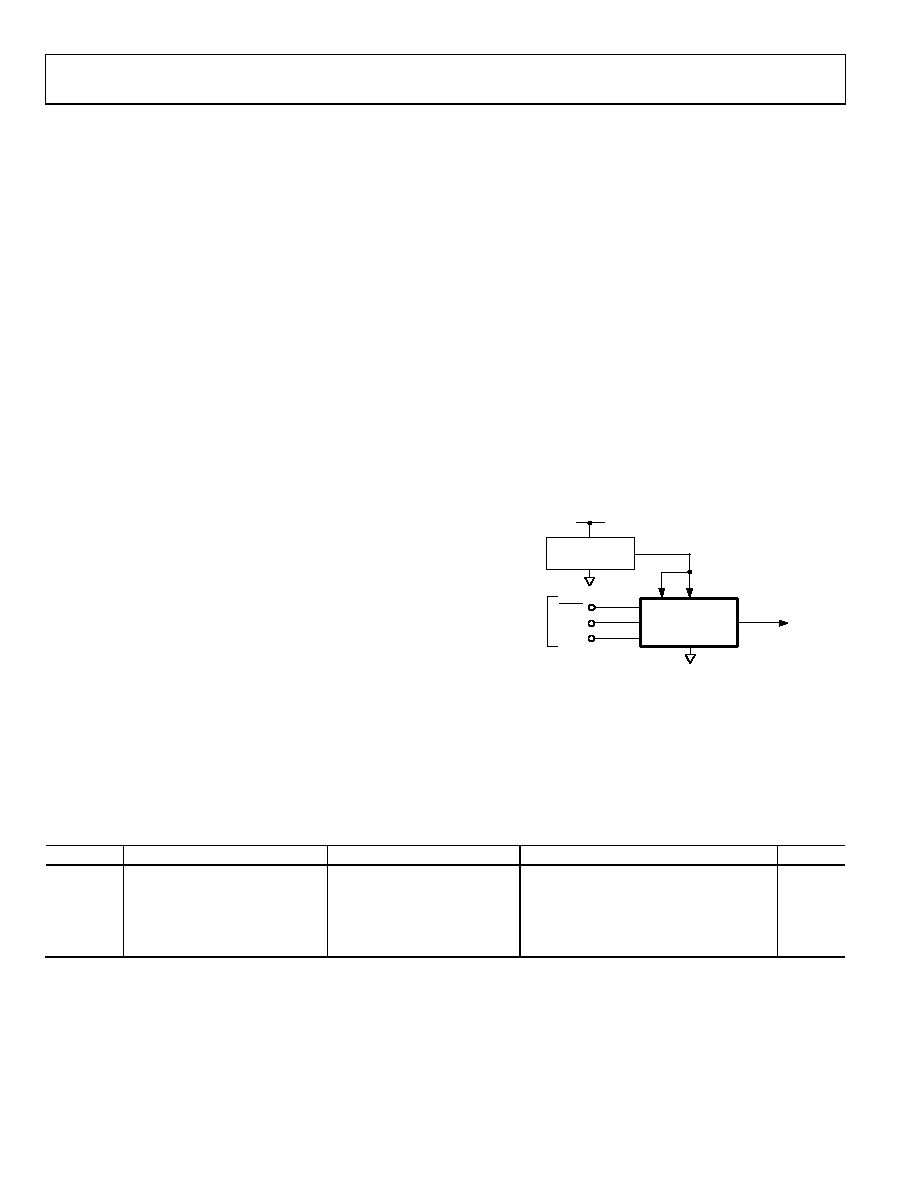
AD5662
3-WIRE
SERIAL
INTERFACE
SYNC
SCLK
DIN
+15V
+5V
250
μA
VOUT = 0V TO 5V
VREF
VDD
REF195
04777-031
Figure 41. REF195 as Power Supply to the AD5662
Table 6. Partial List of Precision References for Use with the AD5662
Part No.
Initial Accuracy (mV max)
Temp Drift (ppm
oC max)
0.1 Hz to 10 Hz Noise (μV p-p typ)
VOUT (V)
ADR425
±2
3
3.4
5
ADR395
±6
25
5
REF195
±2
5
50
5
AD780
±2
3
4
2.5/3
ADR423
±2
3
3.4
3
相关PDF资料 |
PDF描述 |
|---|---|
| AD5439YRU | IC DAC DUAL 10BIT MULT 16-TSSOP |
| SY89834UMI | IC CLK BUF MUX TRNSLA 2:4 16-MLF |
| AD5060ARJZ-2REEL7 | IC DAC 16BIT SPI/SRL SOT23-8 |
| VI-J0V-MY | CONVERTER MOD DC/DC 5.8V 50W |
| VE-JTK-MX-B1 | CONVERTER MOD DC/DC 40V 75W |
相关代理商/技术参数 |
参数描述 |
|---|---|
| AD5662ARM-1REEL7 | 功能描述:IC DAC 16BIT BUFF V-OUT 8-MSOP RoHS:否 类别:集成电路 (IC) >> 数据采集 - 数模转换器 系列:nanoDAC™ 产品培训模块:LTC263x 12-, 10-, and 8-Bit VOUT DAC Family 特色产品:LTC2636 - Octal 12-/10-/8-Bit SPI VOUT DACs with 10ppm/°C Reference 标准包装:91 系列:- 设置时间:4µs 位数:10 数据接口:MICROWIRE?,串行,SPI? 转换器数目:8 电压电源:单电源 功率耗散(最大):2.7mW 工作温度:-40°C ~ 85°C 安装类型:表面贴装 封装/外壳:14-WFDFN 裸露焊盘 供应商设备封装:14-DFN-EP(4x3) 包装:管件 输出数目和类型:8 电压,单极 采样率(每秒):* |
| AD5662ARMZ-1 | 功能描述:IC DAC 16BIT BUFF V-OUT 8-MSOP RoHS:是 类别:集成电路 (IC) >> 数据采集 - 数模转换器 系列:nanoDAC™ 产品培训模块:Lead (SnPb) Finish for COTS Obsolescence Mitigation Program 标准包装:50 系列:- 设置时间:4µs 位数:12 数据接口:串行 转换器数目:2 电压电源:单电源 功率耗散(最大):- 工作温度:-40°C ~ 85°C 安装类型:表面贴装 封装/外壳:8-TSSOP,8-MSOP(0.118",3.00mm 宽) 供应商设备封装:8-uMAX 包装:管件 输出数目和类型:2 电压,单极 采样率(每秒):* 产品目录页面:1398 (CN2011-ZH PDF) |
| AD5662ARMZ-1REEL7 | 功能描述:IC DAC 16BIT SGL 3/5V 8-MSOP RoHS:是 类别:集成电路 (IC) >> 数据采集 - 数模转换器 系列:nanoDAC™ 产品培训模块:LTC263x 12-, 10-, and 8-Bit VOUT DAC Family 特色产品:LTC2636 - Octal 12-/10-/8-Bit SPI VOUT DACs with 10ppm/°C Reference 标准包装:91 系列:- 设置时间:4µs 位数:10 数据接口:MICROWIRE?,串行,SPI? 转换器数目:8 电压电源:单电源 功率耗散(最大):2.7mW 工作温度:-40°C ~ 85°C 安装类型:表面贴装 封装/外壳:14-WFDFN 裸露焊盘 供应商设备封装:14-DFN-EP(4x3) 包装:管件 输出数目和类型:8 电压,单极 采样率(每秒):* |
| AD5662BRJ-1 | 制造商:AD 制造商全称:Analog Devices 功能描述:2.7 V to 5.5 V, 250 ??A, Rail-to-Rail Output 16-Bit DAC D/A in a SOT-23 |
| AD5662BRJ-1500RL7 | 功能描述:IC DAC 16BIT BUFF V-OUT SOT23-8 RoHS:否 类别:集成电路 (IC) >> 数据采集 - 数模转换器 系列:nanoDAC™ 产品培训模块:LTC263x 12-, 10-, and 8-Bit VOUT DAC Family 特色产品:LTC2636 - Octal 12-/10-/8-Bit SPI VOUT DACs with 10ppm/°C Reference 标准包装:91 系列:- 设置时间:4µs 位数:10 数据接口:MICROWIRE?,串行,SPI? 转换器数目:8 电压电源:单电源 功率耗散(最大):2.7mW 工作温度:-40°C ~ 85°C 安装类型:表面贴装 封装/外壳:14-WFDFN 裸露焊盘 供应商设备封装:14-DFN-EP(4x3) 包装:管件 输出数目和类型:8 电压,单极 采样率(每秒):* |
发布紧急采购,3分钟左右您将得到回复。