参数资料
| 型号: | AD5662ARMZ-1 |
| 厂商: | Analog Devices Inc |
| 文件页数: | 8/24页 |
| 文件大小: | 0K |
| 描述: | IC DAC 16BIT BUFF V-OUT 8-MSOP |
| 产品培训模块: | Data Converter Fundamentals DAC Architectures |
| 设计资源: | 4 mA to 20 mA Process Control Loop Using AD5662 (CN0009) 16-Bit Fully Isolated Voltage Output Module Using AD5662, ADuM1401, and External Amplifiers (CN0063) 16-Bit Fully Isolated 4 mA to 20 mA Output Module Using AD5662, ADuM1401, and External Amplifiers (CN0064) |
| 标准包装: | 50 |
| 系列: | nanoDAC™ |
| 设置时间: | 8µs |
| 位数: | 16 |
| 数据接口: | DSP,MICROWIRE?,QSPI?,串行,SPI? |
| 转换器数目: | 1 |
| 电压电源: | 单电源 |
| 工作温度: | -40°C ~ 125°C |
| 安装类型: | 表面贴装 |
| 封装/外壳: | 8-TSSOP,8-MSOP(0.118",3.00mm 宽) |
| 供应商设备封装: | 8-MSOP |
| 包装: | 管件 |
| 输出数目和类型: | 1 电压,单极 |
| 产品目录页面: | 783 (CN2011-ZH PDF) |
AD5662
Rev. A | Page 16 of 24
POWER-DOWN MODES
The AD5662 contains four separate modes of operation. These
modes are software-programmable by setting two bits (DB17
and DB16) in the control register. Table 5 shows how the state
of the bits corresponds to the device’s mode of operation.
Table 5. Modes of Operation for the AD5662
DB17
DB16
Operating Mode
0
Normal Operation
Power-Down Modes
0
1
1 kΩ to GND
1
0
100 kΩ to GND
1
Three-State
When both bits are set to 0, the part works normally with its
normal power consumption of 250 μA at 5 V. However, for the
three power-down modes, the supply current falls to 480 nA at
5 V (100 nA at 3 V). Not only does the supply current fall, but
the output stage is also internally switched from the output of
the amplifier to a resistor network of known values. This has the
advantage that the output impedance of the part is known while
the part is in power-down mode. The outputs can either be
connected internally to GND through a 1 kΩ or 100 kΩ
resistor, or left open-circuited (three-state) (see Figure 36).
RESISTOR
NETWORK
VOUT
RESISTOR
STRING DAC
04777-026
POWER-DOWN
CIRCUITRY
AMPLIFIER
Figure 36. Output Stage During Power-Down
The bias generator, the output amplifier, the resistor string, and
other associated linear circuitry are shut down when power-
down mode is activated. However, the contents of the DAC
register are unaffected when in power-down. The time to exit
power-down is typically 4 μs for VDD = 5 V and for VDD = 3 V
(see Figure 24).
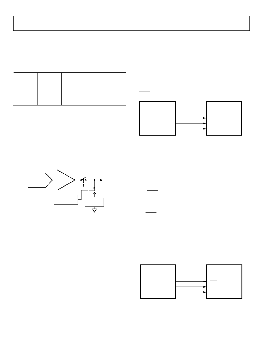
MICROPROCESSOR INTERFACING
AD5662 to Blackfin ADSP-BF53x Interface
Figure 37 shows a serial interface between the AD5662 and
the Blackfin ADSP-BF53x microprocessor. The ADSP-BF53x
processor family incorporates two dual-channel synchronous
serial ports, SPORT1 and SPORT0, for serial and multiprocessor
communications. Using SPORT0 to connect to the AD5662, the
setup for the interface is as follows. DT0PRI drives the DIN pin
of the AD5662, while TSCLK0 drives the SCLK of the part. The
SYNC is driven from TFS0.
AD5662*
*ADDITIONAL PINS OMITTED FOR CLARITY
TFS0
DTOPRI
TSCLK0
SYNC
DIN
SCLK
04777-027
ADSP-BF53x*
Figure 37. AD5662 to Blackfin ADSP-BF53x Interface
AD5662 to 68HC11/68L11 Interface
Figure 38 shows a serial interface between the AD5662 and the
68HC11/68L11 microcontroller. SCK of the 68HC11/68L11
drives the SCLK of the AD5662, while the MOSI output drives
the serial data line of the DAC.
The SYNC signal is derived from a port line (PC7). The setup
conditions for correct operation of this interface are as follows.
The 68HC11/68L11 is configured with its CPOL bit as a 0 and
its CPHA bit as a 1. When data is being transmitted to the DAC,
the SYNC line is taken low (PC7). When the 68HC11/ 68L11 is
configured as described above, data appearing on the MOSI
output is valid on the falling edge of SCK. Serial data from the
68HC11/68L11 is transmitted in 8-bit bytes with only eight
falling clock edges occurring in the transmit cycle. Data is
transmitted MSB first. In order to load data to the AD5662, PC7
is left low after the first eight bits are transferred, and a second
serial write operation is performed to the DAC; PC7 is taken
high at the end of this procedure.
AD5662*
*ADDITIONAL PINS OMITTED FOR CLARITY
PC7
SCK
MOSI
SYNC
SCLK
DIN
04777-028
68HC11/68L11*
Figure 38. AD5662 to 68HC11/68L11 Interface
相关PDF资料 |
PDF描述 |
|---|---|
| VI-2N0-MW-F3 | CONVERTER MOD DC/DC 5V 100W |
| VI-202-MY-F3 | CONVERTER MOD DC/DC 15V 50W |
| VI-2N0-MW-F2 | CONVERTER MOD DC/DC 5V 100W |
| AD5308ARUZ | IC DAC 8BIT OCTAL W/BUFF 16TSSOP |
| VI-202-MY-F2 | CONVERTER MOD DC/DC 15V 50W |
相关代理商/技术参数 |
参数描述 |
|---|---|
| AD5662ARMZ-1REEL7 | 功能描述:IC DAC 16BIT SGL 3/5V 8-MSOP RoHS:是 类别:集成电路 (IC) >> 数据采集 - 数模转换器 系列:nanoDAC™ 产品培训模块:LTC263x 12-, 10-, and 8-Bit VOUT DAC Family 特色产品:LTC2636 - Octal 12-/10-/8-Bit SPI VOUT DACs with 10ppm/°C Reference 标准包装:91 系列:- 设置时间:4µs 位数:10 数据接口:MICROWIRE?,串行,SPI? 转换器数目:8 电压电源:单电源 功率耗散(最大):2.7mW 工作温度:-40°C ~ 85°C 安装类型:表面贴装 封装/外壳:14-WFDFN 裸露焊盘 供应商设备封装:14-DFN-EP(4x3) 包装:管件 输出数目和类型:8 电压,单极 采样率(每秒):* |
| AD5662BRJ-1 | 制造商:AD 制造商全称:Analog Devices 功能描述:2.7 V to 5.5 V, 250 ??A, Rail-to-Rail Output 16-Bit DAC D/A in a SOT-23 |
| AD5662BRJ-1500RL7 | 功能描述:IC DAC 16BIT BUFF V-OUT SOT23-8 RoHS:否 类别:集成电路 (IC) >> 数据采集 - 数模转换器 系列:nanoDAC™ 产品培训模块:LTC263x 12-, 10-, and 8-Bit VOUT DAC Family 特色产品:LTC2636 - Octal 12-/10-/8-Bit SPI VOUT DACs with 10ppm/°C Reference 标准包装:91 系列:- 设置时间:4µs 位数:10 数据接口:MICROWIRE?,串行,SPI? 转换器数目:8 电压电源:单电源 功率耗散(最大):2.7mW 工作温度:-40°C ~ 85°C 安装类型:表面贴装 封装/外壳:14-WFDFN 裸露焊盘 供应商设备封装:14-DFN-EP(4x3) 包装:管件 输出数目和类型:8 电压,单极 采样率(每秒):* |
| AD5662BRJ-1REEL7 | 功能描述:IC DAC 16BIT BUFF V-OUT SOT23-8 RoHS:否 类别:集成电路 (IC) >> 数据采集 - 数模转换器 系列:nanoDAC™ 产品培训模块:LTC263x 12-, 10-, and 8-Bit VOUT DAC Family 特色产品:LTC2636 - Octal 12-/10-/8-Bit SPI VOUT DACs with 10ppm/°C Reference 标准包装:91 系列:- 设置时间:4µs 位数:10 数据接口:MICROWIRE?,串行,SPI? 转换器数目:8 电压电源:单电源 功率耗散(最大):2.7mW 工作温度:-40°C ~ 85°C 安装类型:表面贴装 封装/外壳:14-WFDFN 裸露焊盘 供应商设备封装:14-DFN-EP(4x3) 包装:管件 输出数目和类型:8 电压,单极 采样率(每秒):* |
| AD5662BRJ-2 | 制造商:AD 制造商全称:Analog Devices 功能描述:2.7 V to 5.5 V, 250 ??A, Rail-to-Rail Output 16-Bit DAC D/A in a SOT-23 |
发布紧急采购,3分钟左右您将得到回复。