参数资料
| 型号: | AD5663BRMZ |
| 厂商: | Analog Devices Inc |
| 文件页数: | 6/24页 |
| 文件大小: | 0K |
| 描述: | IC DAC NANO 16BIT DUAL 10-MSOP |
| 产品培训模块: | Data Converter Fundamentals DAC Architectures |
| 标准包装: | 50 |
| 系列: | nanoDAC™ |
| 设置时间: | 4µs |
| 位数: | 16 |
| 数据接口: | 串行 |
| 转换器数目: | 2 |
| 电压电源: | 单电源 |
| 功率耗散(最大): | 2.5mW |
| 工作温度: | -40°C ~ 105°C |
| 安装类型: | 表面贴装 |
| 封装/外壳: | 10-TFSOP,10-MSOP(0.118",3.00mm 宽) |
| 供应商设备封装: | 10-MSOP |
| 包装: | 管件 |
| 输出数目和类型: | 2 电压,单极;2 电压,双极 |
| 采样率(每秒): | 220k |
| 产品目录页面: | 783 (CN2011-ZH PDF) |
| 配用: | EVAL-AD5663REBZ-ND - BOARD EVAL FOR AD5663 |
AD5663
Rev. 0 | Page 14 of 24
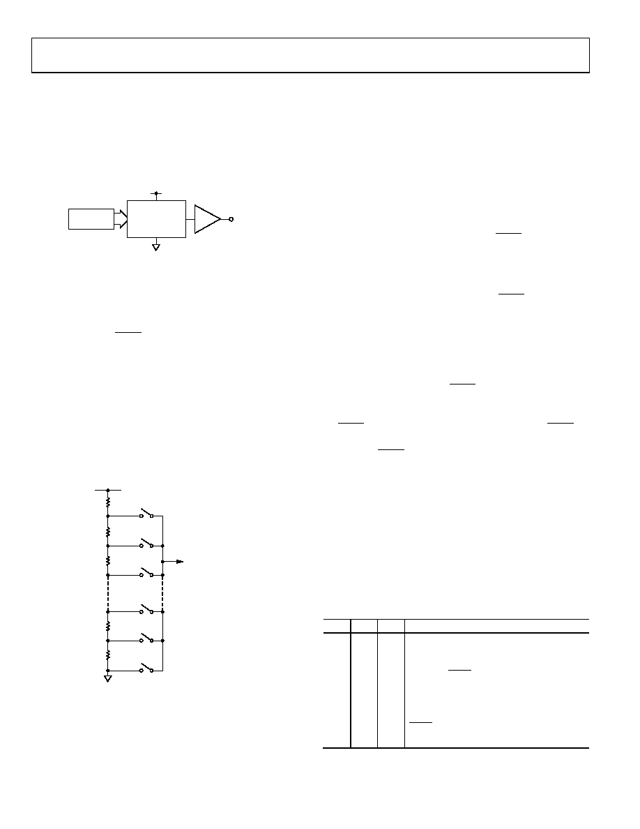
THEORY OF OPERATION
D/A SECTION
The AD5663 DAC is fabricated on a CMOS process. The
architecture consists of a string DAC followed by an output
buffer amplifier. Figure 27 shows a block diagram of the DAC
architecture.
DAC
REGISTER
RESISTOR
STRING
REF (+)
VDD
GND
REF (–)
VOUT
OUTPUT
AMPLIFIER
(GAIN = +2)
0
585
5-
0
32
Figure 27. DAC Architecture
Because the input coding to the DAC is straight binary, the ideal
output voltage is given by
×
=
65,536
D
V
REF
OUT
where D is the decimal equivalent of the binary code that is
loaded to the DAC register. It can range from 0 to 65,535.
RESISTOR STRING
The resistor string section is shown in Figure 28. It is a string of
resistors, each of Value R. The code loaded to the DAC register
determines at which node on the string the voltage is tapped off
to be fed into the output amplifier. The voltage is tapped off by
closing one of the switches connecting the string to the amplifier.
Because it is a string of resistors, it is guaranteed monotonic.
R
TO OUTPUT
AMPLIFIER
0
58
55
-0
33
Figure 28. Resistor String
OUTPUT AMPLIFIER
The output buffer amplifier can generate rail-to-rail voltages on
its output, which gives an output range of 0 V to VDD. It can drive
a load of 2 kΩ in parallel with 1000 pF to GND.
The source and sink capabilities of the output amplifier can be
seen in Figure 14. The slew rate is 1.8 V/μs with a 1/4 to 3/4
full-scale settling time of 10 μs.
SERIAL INTERFACE
The AD5663 has a 3-wire serial interface (SYNC, SCLK, and
DIN) that is compatible with SPI, QSPI, and MICROWIRE
interface standards, as well as with most DSPs. See Figure 2 for
a timing diagram of a typical write sequence.
The write sequence begins by bringing the SYNC line low. Data
from the DIN line is clocked into the 24-bit shift register on the
falling edge of SCLK. The serial clock frequency can be as high
as 50 MHz, making the AD5663 compatible with high speed
DSPs. On the 24th falling clock edge, the last data bit is clocked
in and the programmed function is executed; that is, there is a
change in DAC register contents and/or a change in the mode
of operation. At this stage, the SYNC line can be kept low or be
brought high. In either case, it must be brought high for a mini-
mum of 15 ns before the next write sequence so that a falling edge
of SYNC can initiate the next write sequence. Because the SYNC
buffer draws more current when VIN = 2.0 V than it does when
VIN = 0.10 V, SYNC should be idled low between write sequences
for even lower power operation. As mentioned previously,
however, it must be brought high again just before the next
write sequence.
INPUT SHIFT REGISTER
The input shift register is 24 bits wide (see Figure 29). The first
two bits are don’t cares. The next three are the Command Bit C2
to Command Bit C0 (see Table 7), followed by the 3-bit DAC
Address A2 to DAC Address A0 (see Table 8), and, finally, the
16-bit data-word. These are transferred to the DAC register on
the 24th falling edge of SCLK.
Table 7. Command Definition
C2
C1
C0
Command
0
Write to input register n
0
1
Update DAC register n
0
1
0
Write to input register n, update all
(software LDAC)
0
1
Write to and update DAC channel n
1
0
Power down DAC (power up)
1
0
1
Reset
1
0
LDAC register setup
1
Reserved
相关PDF资料 |
PDF描述 |
|---|---|
| VI-B4L-MY-F3 | CONVERTER MOD DC/DC 28V 50W |
| MS27505E13B35SLC | CONN HSG RCPT 22POS BOX MT SCKT |
| AD1933WBSTZ | IC DAC 24BIT SRL/SPI 64LQFP |
| MS3450W32-6SX | CONN RCPT 23POS WALL MNT W/SCKT |
| AD7533JNZ | IC DAC 10BIT MULTIPLYING 16-DIP |
相关代理商/技术参数 |
参数描述 |
|---|---|
| AD5663BRMZ-1 | 功能描述:IC DAC NANO 16BIT DUAL 10-MSOP RoHS:是 类别:集成电路 (IC) >> 数据采集 - 数模转换器 系列:nanoDAC™ 产品培训模块:Lead (SnPb) Finish for COTS Obsolescence Mitigation Program 标准包装:50 系列:- 设置时间:4µs 位数:12 数据接口:串行 转换器数目:2 电压电源:单电源 功率耗散(最大):- 工作温度:-40°C ~ 85°C 安装类型:表面贴装 封装/外壳:8-TSSOP,8-MSOP(0.118",3.00mm 宽) 供应商设备封装:8-uMAX 包装:管件 输出数目和类型:2 电压,单极 采样率(每秒):* 产品目录页面:1398 (CN2011-ZH PDF) |
| AD5663BRMZ-1REEL7 | 功能描述:IC DAC 16BIT DUAL 10-MSOP RoHS:是 类别:集成电路 (IC) >> 数据采集 - 数模转换器 系列:nanoDAC™ 产品培训模块:LTC263x 12-, 10-, and 8-Bit VOUT DAC Family 特色产品:LTC2636 - Octal 12-/10-/8-Bit SPI VOUT DACs with 10ppm/°C Reference 标准包装:91 系列:- 设置时间:4µs 位数:10 数据接口:MICROWIRE?,串行,SPI? 转换器数目:8 电压电源:单电源 功率耗散(最大):2.7mW 工作温度:-40°C ~ 85°C 安装类型:表面贴装 封装/外壳:14-WFDFN 裸露焊盘 供应商设备封装:14-DFN-EP(4x3) 包装:管件 输出数目和类型:8 电压,单极 采样率(每秒):* |
| AD5663BRMZ-REEL7 | 功能描述:IC DAC 16BIT DUAL 10-MSOP RoHS:是 类别:集成电路 (IC) >> 数据采集 - 数模转换器 系列:nanoDAC™ 产品培训模块:LTC263x 12-, 10-, and 8-Bit VOUT DAC Family 特色产品:LTC2636 - Octal 12-/10-/8-Bit SPI VOUT DACs with 10ppm/°C Reference 标准包装:91 系列:- 设置时间:4µs 位数:10 数据接口:MICROWIRE?,串行,SPI? 转换器数目:8 电压电源:单电源 功率耗散(最大):2.7mW 工作温度:-40°C ~ 85°C 安装类型:表面贴装 封装/外壳:14-WFDFN 裸露焊盘 供应商设备封装:14-DFN-EP(4x3) 包装:管件 输出数目和类型:8 电压,单极 采样率(每秒):* |
| AD5663R | 制造商:AD 制造商全称:Analog Devices 功能描述:Dual 12-/14-/16-Bit nanoDAC with 5 ppm/C On-Chip Reference |
| AD5663RBCPZ-3R2 | 功能描述:IC DAC NANO 16BIT DUAL 10-LFCSP RoHS:是 类别:集成电路 (IC) >> 数据采集 - 数模转换器 系列:nanoDAC™ 标准包装:47 系列:- 设置时间:2µs 位数:14 数据接口:并联 转换器数目:1 电压电源:单电源 功率耗散(最大):55µW 工作温度:-40°C ~ 85°C 安装类型:表面贴装 封装/外壳:28-SSOP(0.209",5.30mm 宽) 供应商设备封装:28-SSOP 包装:管件 输出数目和类型:1 电流,单极;1 电流,双极 采样率(每秒):* |
发布紧急采购,3分钟左右您将得到回复。