参数资料
| 型号: | AD5664ARMZ |
| 厂商: | Analog Devices Inc |
| 文件页数: | 11/24页 |
| 文件大小: | 0K |
| 描述: | IC DAC NANO 16BIT QUAD 10-MSOP |
| 产品培训模块: | Data Converter Fundamentals DAC Architectures |
| 标准包装: | 50 |
| 系列: | nanoDAC™ |
| 设置时间: | 4µs |
| 位数: | 16 |
| 数据接口: | DSP,MICROWIRE?,QSPI?,串行,SPI? |
| 转换器数目: | 4 |
| 电压电源: | 单电源 |
| 工作温度: | -40°C ~ 105°C |
| 安装类型: | 表面贴装 |
| 封装/外壳: | 10-TFSOP,10-MSOP(0.118",3.00mm 宽) |
| 供应商设备封装: | 10-MSOP |
| 包装: | 管件 |
| 输出数目和类型: | 4 电压,单极;4 电压,双极 |
| 采样率(每秒): | 223k |
| 产品目录页面: | 783 (CN2011-ZH PDF) |
| 配用: | EVAL-AD5664REBZ-ND - BOARD EVALUATION FOR AD5664R |
AD5624/AD5664
Rev. 0 | Page 19 of 24
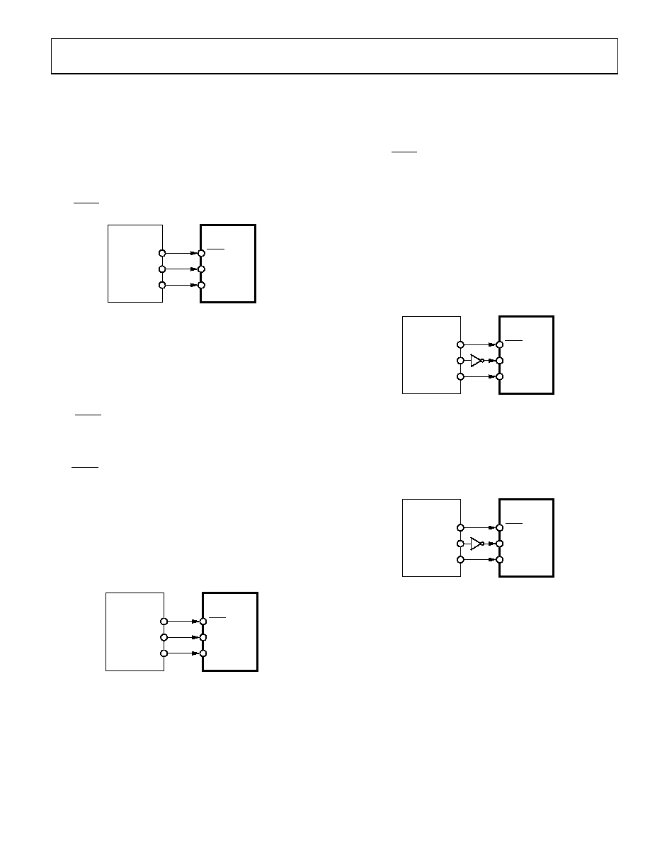
MICROPROCESSOR INTERFACING
AD5624/AD5664 to Blackfin ADSP-BF53x Interface
Figure 35 shows a serial interface between the AD5624/AD5664 and
the Blackfin ADSP-BF53x microprocessor. The ADSP-BF53x
processor family incorporates two dual-channel synchronous serial
ports, SPORT1 and SPORT0, for serial and multiprocessor commu-
nications. Using SPORT0 to connect to the AD5624/AD5664, the
setup for the interface is as follows. DTOPRI drives the DIN pin of
the AD5624/AD5664, while TSCLK0 drives the SCLK of the part.
The SYNC is driven from TFS0.
AD5624/
AD56641
ADSP-BF53x1
SYNC
TFS0
DIN
DTOPRI
SCLK
TSCLK0
1ADDITIONAL PINS OMITTED FOR CLARITY.
05
94
3-
0
38
Figure 35. Blackfin ADSP-BF53x Interface to AD5624/AD5664
AD5624/AD5664 to 68HC11/68L11 Interface
Figure 36 shows a serial interface between the AD5624/AD5664
and the 68HC11/68L11 microcontroller. SCK of the 68HC11/
68L11 drives the SCLK of the AD5624/AD5664, while the
MOSI output drives the serial data line of the DAC.
The SYNC signal is derived from a port line (PC7). The setup
conditions for correct operation of this interface are as follows.
The 68HC11/68L11 is configured with its CPOL bit as a 0 and
its CPHA bit as a 1. When data is being transmitted to the DAC,
the SYNC line is taken low (PC7). When the 68HC11/68L11 is
configured as described previously, data appearing on the MOSI
output is valid on the falling edge of SCK. Serial data from the
68HC11/68L11 is transmitted in 10-bit bytes with only eight
falling clock edges occurring in the transmit cycle. Data is
transmitted MSB first. To load data to the AD5624/AD5664,
PC7 is left low after the first eight bits are transferred, and a
second serial write operation is performed to the DAC; PC7 is
taken high at the end of this procedure.
AD5624/
AD56641
68HC11/68L111
SYNC
PC7
SCLK
SCK
DIN
MOSI
1ADDITIONAL PINS OMITTED FOR CLARITY.
05
94
3-
0
3
9
Figure 36. 68HC11/68L11 Interface to AD5624/AD5664
AD5624/AD5664 to 80C51/80L51 Interface
Figure 37 shows a serial interface between the AD5624/AD5664
and the 80C51/80L51 microcontroller. The setup for the interface
is as follows. TxD of the 80C51/80L51 drives SCLK of the
AD5624/AD5664, while RxD drives the serial data line of the
part. The SYNC signal is derived from a bit-programmable pin
on the port. In this case, port line P3.3 is used. When data is
transmitted to the AD5624/AD5664, P3.3 is taken low. The
80C51/80L51 transmits data in 10-bit bytes only; thus only eight
falling clock edges occur in the transmit cycle. To load data to the
DAC, P3.3 is left low after the first eight bits are transmitted, and
a second write cycle is initiated to transmit the second byte of
data. P3.3 is taken high following the completion of this cycle.
The 80C51/80L51 output the serial data in a format that has the
LSB first. The AD5624/AD5664 must receive data with the MSB
first. The 80C51/80L51 transmit routine should take this into
account.
AD5624/
AD56641
80C51/80L511
SYNC
P3.3
SCLK
TxD
DIN
RxD
1ADDITIONAL PINS OMITTED FOR CLARITY.
05
94
3-
0
4
0
Figure 37. 80C51/80L51 Interface to AD5624/AD5664
AD5624/AD5664 to MICROWIRE Interface
Figure 38 shows an interface between the AD5624/AD5664 and
any MICROWIRE-compatible device. Serial data is shifted out
on the falling edge of the serial clock and is clocked into the
AD5624/AD5664 on the rising edge of the SK.
AD5624/
AD56641
MICROWIRE1
SYNC
CS
SCLK
SK
DIN
SO
1ADDITIONAL PINS OMITTED FOR CLARITY.
05
94
3-
0
4
1
Figure 38. MICROWIRE Interface to AD5624/AD5664
相关PDF资料 |
PDF描述 |
|---|---|
| MS27473T24F2SB | CONN PLUG 100POS STRAIGHT W/SCKT |
| LTC1446CN8#PBF | IC D/A CONV 12BIT R-R DUAL 8-DIP |
| MS3454W16-10P | CONN RCPT 3POS JAM NUT W/PINS |
| LTC1448CN8#PBF | IC D/A CONV 12BIT R-R DUAL 8-DIP |
| AD5062BRJZ-1500RL7 | IC DAC 16BIT 2.7-5.5V SOT23-8 |
相关代理商/技术参数 |
参数描述 |
|---|---|
| AD5664ARMZ-REEL7 | 功能描述:IC DAC 16BIT QUAD 10-MSOP RoHS:是 类别:集成电路 (IC) >> 数据采集 - 数模转换器 系列:nanoDAC™ 标准包装:47 系列:- 设置时间:2µs 位数:14 数据接口:并联 转换器数目:1 电压电源:单电源 功率耗散(最大):55µW 工作温度:-40°C ~ 85°C 安装类型:表面贴装 封装/外壳:28-SSOP(0.209",5.30mm 宽) 供应商设备封装:28-SSOP 包装:管件 输出数目和类型:1 电流,单极;1 电流,双极 采样率(每秒):* |
| AD5664BCPZ-250RL7 | 制造商:AD 制造商全称:Analog Devices 功能描述:2.7 V to 5.5 V, 450 レA, Rail-to-Rail Output, Quad, 12-/16-Bit nanoDACs |
| AD5664BCPZ-R2 | 功能描述:IC DAC NANO 16BIT QUAD 10-LFCSP RoHS:是 类别:集成电路 (IC) >> 数据采集 - 数模转换器 系列:nanoDAC™ 标准包装:47 系列:- 设置时间:2µs 位数:14 数据接口:并联 转换器数目:1 电压电源:单电源 功率耗散(最大):55µW 工作温度:-40°C ~ 85°C 安装类型:表面贴装 封装/外壳:28-SSOP(0.209",5.30mm 宽) 供应商设备封装:28-SSOP 包装:管件 输出数目和类型:1 电流,单极;1 电流,双极 采样率(每秒):* |
| AD5664BCPZ-REEL7 | 功能描述:IC DAC NANO 16BIT QUAD 10-LFCSP RoHS:是 类别:集成电路 (IC) >> 数据采集 - 数模转换器 系列:nanoDAC™ 产品培训模块:Lead (SnPb) Finish for COTS Obsolescence Mitigation Program 标准包装:50 系列:- 设置时间:4µs 位数:12 数据接口:串行 转换器数目:2 电压电源:单电源 功率耗散(最大):- 工作温度:-40°C ~ 85°C 安装类型:表面贴装 封装/外壳:8-TSSOP,8-MSOP(0.118",3.00mm 宽) 供应商设备封装:8-uMAX 包装:管件 输出数目和类型:2 电压,单极 采样率(每秒):* 产品目录页面:1398 (CN2011-ZH PDF) |
| AD5664BRMZ | 功能描述:IC DAC NANO 16BIT QUAD 10-MSOP RoHS:是 类别:集成电路 (IC) >> 数据采集 - 数模转换器 系列:nanoDAC™ 产品培训模块:Lead (SnPb) Finish for COTS Obsolescence Mitigation Program 标准包装:50 系列:- 设置时间:4µs 位数:12 数据接口:串行 转换器数目:2 电压电源:单电源 功率耗散(最大):- 工作温度:-40°C ~ 85°C 安装类型:表面贴装 封装/外壳:8-TSSOP,8-MSOP(0.118",3.00mm 宽) 供应商设备封装:8-uMAX 包装:管件 输出数目和类型:2 电压,单极 采样率(每秒):* 产品目录页面:1398 (CN2011-ZH PDF) |
发布紧急采购,3分钟左右您将得到回复。