参数资料
| 型号: | AD568JQ |
| 厂商: | Analog Devices Inc |
| 文件页数: | 8/14页 |
| 文件大小: | 0K |
| 描述: | IC DAC 12BIT HS MONO 35NS 24CDIP |
| 产品培训模块: | Data Converter Fundamentals DAC Architectures |
| 标准包装: | 1 |
| 设置时间: | 35ns |
| 位数: | 12 |
| 数据接口: | 并联 |
| 转换器数目: | 1 |
| 电压电源: | 双 ± |
| 工作温度: | 0°C ~ 70°C |
| 安装类型: | 通孔 |
| 封装/外壳: | 24-CDIP(0.300",7.62mm) |
| 供应商设备封装: | 24-CDIP |
| 包装: | 管件 |
| 输出数目和类型: | 1 电流,单极;1 电流,双极;1 电压,单极;1 电压,双极 |
| 采样率(每秒): | * |
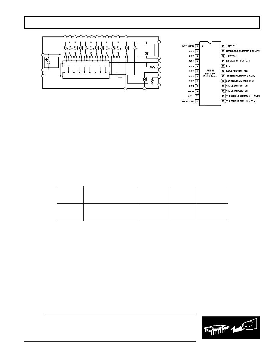
AD568
REV. A
–3–
ORDERING GUIDE
Linearity
Voltage
Temperature
Error Max
Gain T.C.
Model
l
Package Option
2
Range C@ 25 C
Max ppm/ C
AD568JQ
24-Lead Cerdip (Q-24)
0 to +70
±1/2
±50
AD568KQ
24-Lead Cerdip (Q-24)
0 to +70
±1/4
±30
AD568SQ
24-Lead Cerdip (Q-24)
–55 to +125
±1/2
±50
NOTES
1For details on grade and package offerings screened in accordance with MIL-STD-883, refer to the Analog Devices
Military Products Databook or current AD568/883B data sheet.
2Q = Cerdip.
Definitions
LINEARITY ERROR (also called INTEGRAL NONLINEAR-
ITY OR INL): Analog Devices defines linearity error as the
maximum deviation of the actual analog output from the ideal
output (a straight line drawn from 0 to FS) for any bit combina-
tion expressed in multiples of 1 LSB. The AD568 is laser
trimmed to 1/4 LSB (0.006% of FS) maximum linearity error at
+25
°C for the K version and 1/2 LSB for the J and S versions.
DIFFERENTIAL LINEARITY ERROR (also called DIFFER-
ENTIAL NONLINEARITY or DNL): DNL is the measure of
the variation in analog value, normalized to full scale, associated
with a 1 LSB change in digital input code. Monotonic behavior
WARNING!
ESD SENSITIVE DEVICE
CAUTION
ESD (electrostatic discharge) sensitive device. Electrostatic charges as high as 4000 V readily
accumulate on the human body and test equipment and can discharge without detection.
Although the AD568 features proprietary ESD protection circuitry, permanent damage may
occur on devices subjected to high energy electrostatic discharges. Therefore, proper ESD
precautions are recommended to avoid performance degradation or loss of functionality.
requires that the differential linearity error not exceed 1 LSB in
the negative direction.
MONOTONICITY: A DAC is said to be monotonic if the out-
put either increases or remains constant as the digital input
increases.
UNIPOLAR OFFSET ERROR: The deviation of the analog
output from the ideal (0 V or 0 mA) when the inputs are set to
all 0s is called unipolar offset error.
BIPOLAR OFFSET ERROR: The deviation of the analog out-
put from the ideal (negative half-scale) when the inputs are set
to all 0s is called bipolar offset error.
18
6
7
8
9
10
11
12
1
2
3
4
5
19
20
23
24
13
14
17
2X
4X
MSB
LSB
PNP
CURRENT
SOURCES
1.4V
BAND-
GAP
REF
THRESHOLD
CONTROL
THRESHOLD
COMMON
LADDER
COMMON
PNP
SWITCHES
DIFFUSED R-2R LADDER
(10 - 20
)
THIN-FILM R-2R LADDER
(100 - 200
)
BIPOLAR
CURRENT
GENERATOR
BURIED
ZENER
REFERENCE
21
22
200
ANALOG
COMMON
V
CC
I
OUT
REFERENCE
COMMON
1k
15
16
LOAD RESISTOR
(R
L)
BIPOLAR
OFFSET (I
BPO)
10V SPAN
RESISTOR
10V SPAN
RESISTOR
I
OUT
I
OUT
AD568
V
EE
Figure 1. Functional Block Diagram
ABSOLUTE MAXIMUM RATINGS
1
VCC to REFCOM . . . . . . . . . . . . . . . . . . . . . . . . 0 V to +18 V
VEE to REFCOM . . . . . . . . . . . . . . . . . . . . . . . . . 0 V to –18 V
REFCOM to LCOM . . . . . . . . . . . . . . . . . +100 mV to –10 V
ACOM to LCOM . . . . . . . . . . . . . . . . . . . . . . . . . . .
±100 mV
THCOM to LCOM . . . . . . . . . . . . . . . . . . . . . . . . . .
±500 mV
SPANs to LCOM . . . . . . . . . . . . . . . . . . . . . . . . . . . . .
±12 V
IBPO to LCOM . . . . . . . . . . . . . . . . . . . . . . . . . . . . . . . . . ± 5 V
IOUT to LCOM . . . . . . . . . . . . . . . . . . . . . . . . . . . –5 V to VTH
Digital Inputs to THCOM . . . . . . . . . . . . . –500 mV to +7.0 V
Voltage Across Span Resistor . . . . . . . . . . . . . . . . . . . . . . 12 V
VTH to THCOM . . . . . . . . . . . . . . . . . . . . . . –0.7 V to +1.4 V
Logic Threshold Control Input Current . . . . . . . . . . . . . 5 mA
Power Dissipation . . . . . . . . . . . . . . . . . . . . . . . . . . . 100 mW
Storage Temperature Range
Q (Cerdip) Package . . . . . . . . . . . . . . . . . –65
°C to +150°C
Junction Temperature . . . . . . . . . . . . . . . . . . . . . . . . . . 175
°C
Thermal Resistance
θ
JA
. . . . . . . . . . . . . . . . . . . . . . . . . . . . . . . . . . . . . . 75
°C/W
θ
JC
. . . . . . . . . . . . . . . . . . . . . . . . . . . . . . . . . . . . . . 25
°C/W
1Stresses above those listed under “Absolute Maximum Ratings” may cause
permanent damage to the device. This is a stress rating only and functional
operation of the device at these or any other conditions above those indicated in the
operational section of this specification is not implied. Exposure to absolute
maximum rating conditions for extended periods may affect device reliability.
PIN CONFIGURATION
相关PDF资料 |
PDF描述 |
|---|---|
| VE-J5J-MZ-B1 | CONVERTER MOD DC/DC 36V 25W |
| AD561JD | IC DAC 10BIT 5-15V IN MONO 16DIP |
| VE-J5H-MZ-B1 | CONVERTER MOD DC/DC 52V 25W |
| VI-JWJ-MZ-B1 | CONVERTER MOD DC/DC 36V 25W |
| AD561KNZ | IC DAC 10BIT MONO VOLT IN 16DIP |
相关代理商/技术参数 |
参数描述 |
|---|---|
| AD568K | 制造商:AD 制造商全称:Analog Devices 功能描述:12-Bit Ultrahigh Speed Monolithic D/A Converter |
| AD568KQ | 功能描述:IC DAC 12BIT HS MONO 35NS 24CDIP RoHS:否 类别:集成电路 (IC) >> 数据采集 - 数模转换器 系列:- 产品培训模块:Lead (SnPb) Finish for COTS Obsolescence Mitigation Program 标准包装:1,000 系列:- 设置时间:1µs 位数:8 数据接口:串行 转换器数目:8 电压电源:双 ± 功率耗散(最大):941mW 工作温度:0°C ~ 70°C 安装类型:表面贴装 封装/外壳:24-SOIC(0.295",7.50mm 宽) 供应商设备封装:24-SOIC W 包装:带卷 (TR) 输出数目和类型:8 电压,单极 采样率(每秒):* |
| AD568S | 制造商:AD 制造商全称:Analog Devices 功能描述:12-Bit Ultrahigh Speed Monolithic D/A Converter |
| AD568SE/883B | 制造商:Rochester Electronics LLC 功能描述:- Bulk 制造商:Analog Devices 功能描述: |
| AD568SQ | 功能描述:数模转换器- DAC IC MONO 12-BIT D/A CONV RoHS:否 制造商:Texas Instruments 转换器数量:1 DAC 输出端数量:1 转换速率:2 MSPs 分辨率:16 bit 接口类型:QSPI, SPI, Serial (3-Wire, Microwire) 稳定时间:1 us 最大工作温度:+ 85 C 安装风格:SMD/SMT 封装 / 箱体:SOIC-14 封装:Tube |
发布紧急采购,3分钟左右您将得到回复。