- 您现在的位置:买卖IC网 > PDF目录8561 > AD569JP-REEL (Analog Devices Inc)IC DAC 16BIT MONO NON-LIN 28PLCC PDF资料下载
参数资料
| 型号: | AD569JP-REEL |
| 厂商: | Analog Devices Inc |
| 文件页数: | 10/12页 |
| 文件大小: | 0K |
| 描述: | IC DAC 16BIT MONO NON-LIN 28PLCC |
| 产品培训模块: | Data Converter Fundamentals DAC Architectures |
| 标准包装: | 750 |
| 设置时间: | 4µs |
| 位数: | 16 |
| 数据接口: | 并联 |
| 转换器数目: | 1 |
| 电压电源: | 双 ± |
| 工作温度: | 0°C ~ 70°C |
| 安装类型: | 表面贴装 |
| 封装/外壳: | 28-LCC(J 形引线) |
| 供应商设备封装: | 28-PLCC(11.51x11.51) |
| 包装: | 带卷 (TR) |
| 输出数目和类型: | 1 电压,单极;1 电压,双极 |
| 采样率(每秒): | * |
AD569
REV. A
–7–
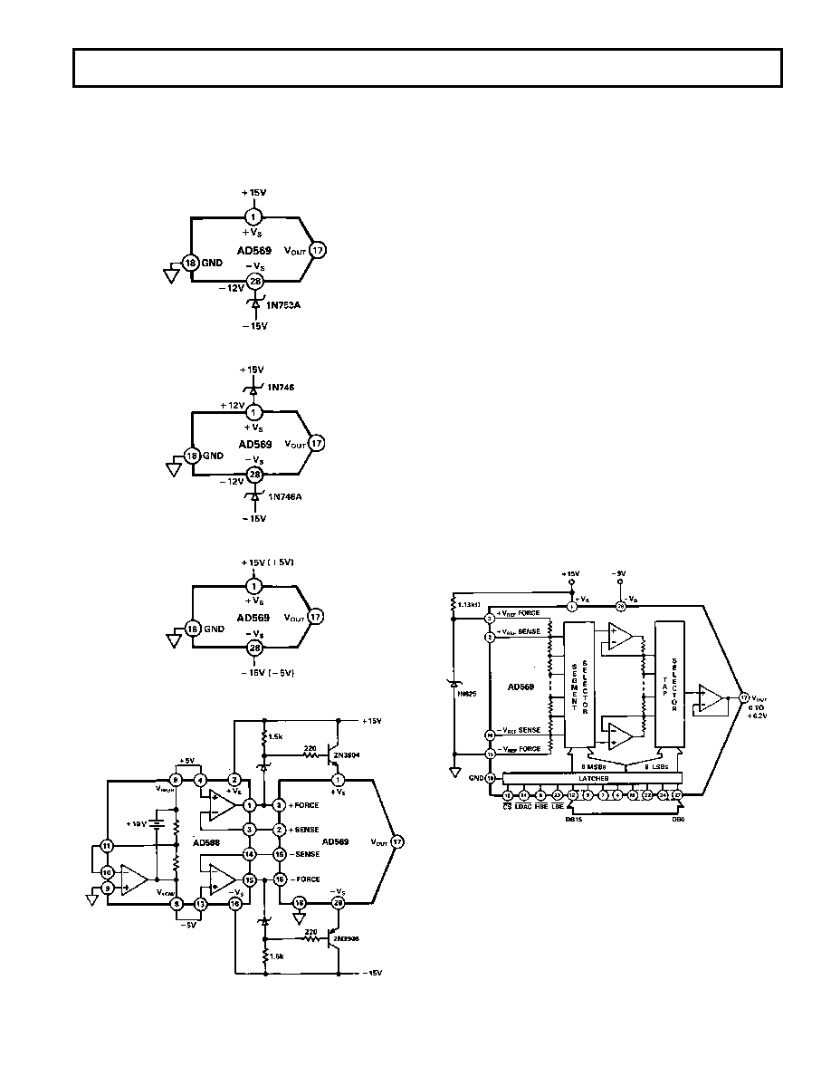
benefit is that, should a Zener diode fail (a short circuit would
be the most likely failure), the supply voltage decreases. This
differs from the situation where the diode is used as a series
regulator. In that case, a failure would place the unregulated
supply voltage on the AD569 terminal.
a. Zener Regulates Negative Supply
b. Diodes Regulate Both Supplies
c. Use of
±15 V and ±5 V Supplies
d. AD588 Produces References and Supply Voltages
Figure 7. Power Supply Options
ANALOG CIRCUIT CONNECTIONS
The AD569 is intended for use in applications where high reso-
lution and stability are critical. Designed as a multiplying D/A
converter, the AD569 may be used with a fixed dc reference or
an ac reference. VREF may be any voltage or combination of
voltages at +VFORCE and –VFORCE that remain within the bounds
set for reference voltages as discussed in the power supply range
section. Since the AD569 is a multiplying D/A converter, its
output voltage, VOUT, is proportional to the product of the digi-
tal input word and the voltage at the reference terminal. The
transfer function is VOUT = DVREF where D is the fractional bi-
nary value of the digital word applied to the converter using
offset-binary coding. Therefore, the output will range from
–VREF for a digital input code of all zeros (0000H) to +VREF for
an input code of all ones (FFFFH).
For applications where absolute accuracy is not critical, the
simple reference connection in Figure 8 can be used. Using only
the reference force inputs, this configuration maintains linearity
and 16-bit monotonicity, but introduces small, fixed offset and
gain errors. These errors are due to the voltage drops across re-
sistors RA and RB shown in Figure 9. With a 10 V reference
voltage, the gain and offset errors will range from 80 mV to
100 mV. Resistors RA and RB were included in the first resistor
string to avoid degraded linearity due to uneven current densi-
ties at the string’s endpoints. Similarly, linearity would degrade
if the reference voltage were connected across the reference
sense terminals. Note that the resistance between the force and
sense terminals cannot be measured with an ohmmeter; the lay-
out of the thin-film resistor string adds approximately 4 k
of
resistance (RS) at the sense tap.
Figure 8. Simple Reference Connection
For those applications in which precision references and high
accuracy are critical, buffer amplifiers are used at +VREF and
–VREF as shown in Figure 10 to force the voltage across resistors
R1 to R256. This insures that any errors induced by currents
flowing through the resistances of the package pins, bond wires,
aluminum interconnections, as well as RA and RB are mini-
mized. Suitable amplifiers are the AD517, AD OP07, AD OP27,
or the dual amplifier, the AD712. Errors will arise, however, as
the buffer amplifiers’ bias currents flow through RS (4 k
). If
the bias currents produce such errors, resistance can be inserted
at the noninverting terminal (RBC) of the buffer amplifiers to
compensate for the errors.
相关PDF资料 |
PDF描述 |
|---|---|
| VI-BW4-MX-S | CONVERTER MOD DC/DC 48V 75W |
| AD7834BR-REEL | IC DAC 14BIT QUAD SRL 28-SOIC |
| VI-B20-MX-S | CONVERTER MOD DC/DC 5V 75W |
| VE-JWK-MW-S | CONVERTER MOD DC/DC 40V 100W |
| MAX5679ETJ+ | IC GENERATOR PROG LCD 32TQFN |
相关代理商/技术参数 |
参数描述 |
|---|---|
| AD569JPZ | 功能描述:IC DAC 16BIT MONO NON-LIN 28PLCC RoHS:是 类别:集成电路 (IC) >> 数据采集 - 数模转换器 系列:- 产品培训模块:Lead (SnPb) Finish for COTS Obsolescence Mitigation Program 标准包装:50 系列:- 设置时间:4µs 位数:12 数据接口:串行 转换器数目:2 电压电源:单电源 功率耗散(最大):- 工作温度:-40°C ~ 85°C 安装类型:表面贴装 封装/外壳:8-TSSOP,8-MSOP(0.118",3.00mm 宽) 供应商设备封装:8-uMAX 包装:管件 输出数目和类型:2 电压,单极 采样率(每秒):* 产品目录页面:1398 (CN2011-ZH PDF) |
| AD569JPZ-REEL | 功能描述:IC DAC 16BIT MONO NON-LIN 28PLCC RoHS:是 类别:集成电路 (IC) >> 数据采集 - 数模转换器 系列:- 产品培训模块:Lead (SnPb) Finish for COTS Obsolescence Mitigation Program 标准包装:1,000 系列:- 设置时间:1µs 位数:8 数据接口:串行 转换器数目:8 电压电源:双 ± 功率耗散(最大):941mW 工作温度:0°C ~ 70°C 安装类型:表面贴装 封装/外壳:24-SOIC(0.295",7.50mm 宽) 供应商设备封装:24-SOIC W 包装:带卷 (TR) 输出数目和类型:8 电压,单极 采样率(每秒):* |
| AD569KN | 功能描述:IC DAC 16BIT MONO NON-LIN 28-DIP RoHS:否 类别:集成电路 (IC) >> 数据采集 - 数模转换器 系列:- 产品培训模块:Lead (SnPb) Finish for COTS Obsolescence Mitigation Program 标准包装:1,000 系列:- 设置时间:1µs 位数:8 数据接口:串行 转换器数目:8 电压电源:双 ± 功率耗散(最大):941mW 工作温度:0°C ~ 70°C 安装类型:表面贴装 封装/外壳:24-SOIC(0.295",7.50mm 宽) 供应商设备封装:24-SOIC W 包装:带卷 (TR) 输出数目和类型:8 电压,单极 采样率(每秒):* |
| AD569KNZ | 功能描述:IC DAC 16BIT MONOTONIC 28-DIP RoHS:是 类别:集成电路 (IC) >> 数据采集 - 数模转换器 系列:- 产品培训模块:Lead (SnPb) Finish for COTS Obsolescence Mitigation Program 标准包装:50 系列:- 设置时间:4µs 位数:12 数据接口:串行 转换器数目:2 电压电源:单电源 功率耗散(最大):- 工作温度:-40°C ~ 85°C 安装类型:表面贴装 封装/外壳:8-TSSOP,8-MSOP(0.118",3.00mm 宽) 供应商设备封装:8-uMAX 包装:管件 输出数目和类型:2 电压,单极 采样率(每秒):* 产品目录页面:1398 (CN2011-ZH PDF) |
| AD569KP | 制造商:Analog Devices 功能描述:DAC 1-CH Resistor-String 16-bit 28-Pin PLCC 制造商:Rochester Electronics LLC 功能描述:IC,MONO 16-BIT D/A CONV - Bulk 制造商:Analog Devices 功能描述:IC SEMICONDUCTOR ((NS)) |
发布紧急采购,3分钟左右您将得到回复。