参数资料
| 型号: | AD569JPZ |
| 厂商: | Analog Devices Inc |
| 文件页数: | 8/12页 |
| 文件大小: | 0K |
| 描述: | IC DAC 16BIT MONO NON-LIN 28PLCC |
| 产品培训模块: | Data Converter Fundamentals DAC Architectures |
| 标准包装: | 1 |
| 设置时间: | 4µs |
| 位数: | 16 |
| 数据接口: | 并联 |
| 转换器数目: | 1 |
| 电压电源: | 双 ± |
| 工作温度: | 0°C ~ 70°C |
| 安装类型: | 表面贴装 |
| 封装/外壳: | 28-LCC(J 形引线) |
| 供应商设备封装: | 28-PLCC(11.51x11.51) |
| 包装: | 管件 |
| 输出数目和类型: | 1 电压,单极;1 电压,双极 |
| 采样率(每秒): | * |
| 产品目录页面: | 781 (CN2011-ZH PDF) |
AD569
REV. A
–5–
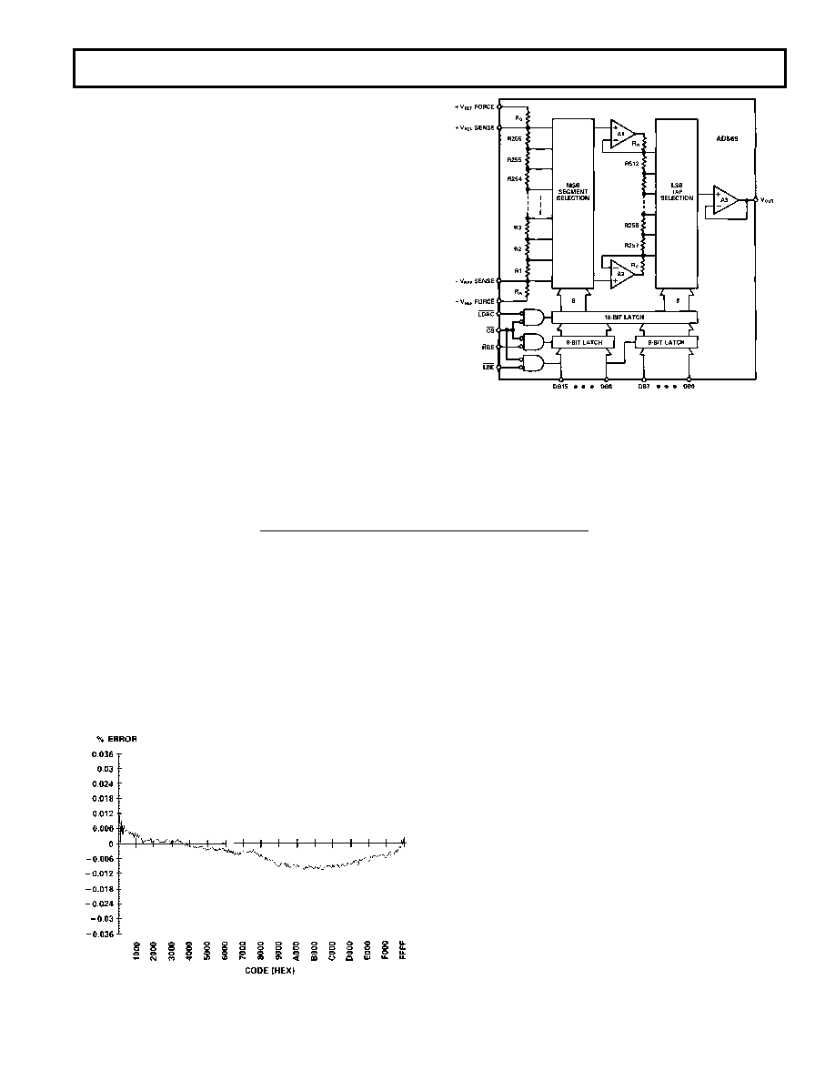
Figure 3. AD569 Block Diagram
FUNCTIONAL DESCRIPTION
The AD569 consists of two resistor strings, each of which is di-
vided into 256 equal segments (see Figure 3). The 8 MSBs of
the digital input word select one of the 256 segments on the first
string. The taps at the top and bottom of the selected segment
are connected to the inputs of the two buffer amplifiers A1 and
A2. These amplifiers exhibit extremely high CMRR and low
bias current, and thus accurately preserve the voltages at the top
and bottom of the segment. The buffered voltages from the seg-
ment endpoints are applied across the second resistor string,
where the 8LSBs of the digital input word select one of the 256
taps. Output amplifier A3 buffers this voltage and delivers it to
the output.
Buffer amplifiers A1 and A2 leap-frog up the first string to pre-
serve monotonicity at the segment boundaries. For example,
when increasing the digital code from 00FFH to 0100H, (the first
segment boundary), A1 remains connected to the same tap on
the first resistor, while A2 jumps over it and is connected to the
tap which becomes the top of the next segment. This design
guarantees monotonicity even if the amplifiers have offset volt-
ages. In fact, amplifier offset only contributes to integral linear-
ity error.
CAUTION
It is generally considered good engineering practice to avoid
inserting integrated circuits into powered-up sockets. This
guideline is especially important with the AD569. An empty,
powered-up socket configures external buffer amplifiers in an
open-loop mode, forcing their outputs to be at the positive or
negative rail. This condition may result in a large current surge
between the reference force and sense terminals. This current
surge may permanently damage the AD569.
ANALOG CIRCUIT DETAILS
MONOTONICITY: A DAC is monotonic if the output either
increases or remains constant for increasing digital inputs. All
versions of the AD569 are monotonic over their full operating
temperature range.
DIFFERENTIAL NONLINEARITY: DNL is the measure of
the change in the analog output, normalized to full scale, associ-
ated: with a 1 LSB change in the digital input code. Monotonic
behavior requires that the differential linearity error be less than
1 LSB over the temperature range of interest. For example, for a
±5 V output range, a change of 1 LSB in digital input code
should result in a 152
V change in the analog output (1 LSB =
10 V/65,536). If the change is actually 38
V, however, the dif-
ferential linearity error would be –114
V, or –3/4 LSB. By leap-
frogging the buffer amplifier taps on the first divider, a typical
AD569 keeps DNL within
±38 V (±1/4 LSB) around each of
the 256 segment boundaries defined by the upper byte of the in-
put word (see Figure 5). Within the second divider, DNL also
typically remains less than
±38 V as shown in Figure 6. Since
the second divider is independent of absolute voltage, DNL is
the same within the rest of the 256 segments.
OFFSET ERROR: The difference between the actual analog
output and the ideal output (–VREF), with the inputs loaded with
all zeros is called the offset error. For the AD569, Unipolar Off-
set is specified with 0 V applied to –VREF and Bipolar Offset is
specified with –5 V applied to –VREF. Either offset is trimmed by
adjusting the voltage applied to the –VREF terminals.
BIPOLAR ZERO ERROR: The deviation of the analog output
from the ideal half-scale output of 0.0000 V when the inputs are
loaded with 8000H is called the Bipolar Zero Error. For the
AD569, it is specified with
±5 V applied to the reference
terminals.
Definitions
LINEARITY ERROR: Analog Devices defines linearity error as
the maximum deviation of the actual, adjusted DAC output
from the ideal output (a straight line drawn from 0 to FS–1LSB)
for any bit combination. The AD569’s linearity is primarily lim-
ited by resistor uniformity in the first divider (upper byte of
16-bit input). The plot in Figure 4 shows the AD569’s typical
linearity error across the entire output range to be within
±0.01% of full scale. At 25°C the maximum linearity error for
the AD569JN, AD and SD grades is specified to be
±0.04%,
and
±0.024% for the KN and BD versions.
Figure 4. Typical Linearity
相关PDF资料 |
PDF描述 |
|---|---|
| AD9146BCPZ | IC DAC 16BIT SRL DUAL 48LFCSP |
| GTC02R-36-5P | CONN RCPT 4POS BOX MNT W/PINS |
| VE-2TY-MX-F2 | CONVERTER MOD DC/DC 3.3V 49.5W |
| MS27508E24B4PC | CONN RCPT 56POS BOX MNT W/PINS |
| VE-2TY-MW-F2 | CONVERTER MOD DC/DC 3.3V 66W |
相关代理商/技术参数 |
参数描述 |
|---|---|
| AD569JPZ-REEL | 功能描述:IC DAC 16BIT MONO NON-LIN 28PLCC RoHS:是 类别:集成电路 (IC) >> 数据采集 - 数模转换器 系列:- 产品培训模块:Lead (SnPb) Finish for COTS Obsolescence Mitigation Program 标准包装:1,000 系列:- 设置时间:1µs 位数:8 数据接口:串行 转换器数目:8 电压电源:双 ± 功率耗散(最大):941mW 工作温度:0°C ~ 70°C 安装类型:表面贴装 封装/外壳:24-SOIC(0.295",7.50mm 宽) 供应商设备封装:24-SOIC W 包装:带卷 (TR) 输出数目和类型:8 电压,单极 采样率(每秒):* |
| AD569KN | 功能描述:IC DAC 16BIT MONO NON-LIN 28-DIP RoHS:否 类别:集成电路 (IC) >> 数据采集 - 数模转换器 系列:- 产品培训模块:Lead (SnPb) Finish for COTS Obsolescence Mitigation Program 标准包装:1,000 系列:- 设置时间:1µs 位数:8 数据接口:串行 转换器数目:8 电压电源:双 ± 功率耗散(最大):941mW 工作温度:0°C ~ 70°C 安装类型:表面贴装 封装/外壳:24-SOIC(0.295",7.50mm 宽) 供应商设备封装:24-SOIC W 包装:带卷 (TR) 输出数目和类型:8 电压,单极 采样率(每秒):* |
| AD569KNZ | 功能描述:IC DAC 16BIT MONOTONIC 28-DIP RoHS:是 类别:集成电路 (IC) >> 数据采集 - 数模转换器 系列:- 产品培训模块:Lead (SnPb) Finish for COTS Obsolescence Mitigation Program 标准包装:50 系列:- 设置时间:4µs 位数:12 数据接口:串行 转换器数目:2 电压电源:单电源 功率耗散(最大):- 工作温度:-40°C ~ 85°C 安装类型:表面贴装 封装/外壳:8-TSSOP,8-MSOP(0.118",3.00mm 宽) 供应商设备封装:8-uMAX 包装:管件 输出数目和类型:2 电压,单极 采样率(每秒):* 产品目录页面:1398 (CN2011-ZH PDF) |
| AD569KP | 制造商:Analog Devices 功能描述:DAC 1-CH Resistor-String 16-bit 28-Pin PLCC 制造商:Rochester Electronics LLC 功能描述:IC,MONO 16-BIT D/A CONV - Bulk 制造商:Analog Devices 功能描述:IC SEMICONDUCTOR ((NS)) |
| AD569KPZ | 功能描述:IC DAC 16BIT MONO NON-LIN 28PLCC RoHS:是 类别:集成电路 (IC) >> 数据采集 - 数模转换器 系列:- 标准包装:1 系列:- 设置时间:4.5µs 位数:12 数据接口:串行,SPI? 转换器数目:1 电压电源:单电源 功率耗散(最大):- 工作温度:-40°C ~ 125°C 安装类型:表面贴装 封装/外壳:8-SOIC(0.154",3.90mm 宽) 供应商设备封装:8-SOICN 包装:剪切带 (CT) 输出数目和类型:1 电压,单极;1 电压,双极 采样率(每秒):* 其它名称:MCP4921T-E/SNCTMCP4921T-E/SNRCTMCP4921T-E/SNRCT-ND |
发布紧急采购,3分钟左右您将得到回复。